


 Knocking Down the Bone Pile: Revamp Your Components with BGA Reballing
 Global Sourcing Spotlight: Balancing Speed and Flexibility Without Sacrificing Control
 SMT Perspectives & Prospects: Artificial Intelligence Part 6: Data Module 1


Akrometrix's Ryan Curry to Discuss PCB Design & Material Warpage Challenges at SMTAI
September 23, 2016 | Akrometrix LLCEstimated reading time: 2 minutes
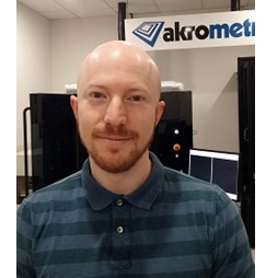
Akrometrix LLC has announced that Ryan Curry, Technical Account Manager, will co-present a paper with Don Adams, Manufacturing Engineering Manager at Bose Corporation, at the SMTA International. The presentation, "Understanding PCB Design and Material Warpage Challenges Which Occur during B2B/Module-Carrier Attachment," is scheduled to take place during session APT7, "Package and PCB Interactions", on Wednesday, September 28 at 4 pm.
PCB warpage has been identified as one of several key contributors to unacceptable yield rates during reflow assembly of a PCB module to a PCB carrier board. The module has a land grid array pattern and is placed directly on solder paste on the carrier board. This results in low-profile solder joints that are sensitive to the co-planarity of both the module and the carrier boards. The typical failure mode occurs when one or more solder joint opens are caused by a lifted corner of the module during/after reflow.
This paper and presentation will present graphical and statistical details of at-room-temperature metrology on a large sample of modules with differing design variables. Shadow Moiré technique will be used to provide accurate warpage profiles of the 6-up module arrays before and after top- and bottom-side assembly, and again before and after attachment to the carrier board. A large volume of samples will be tested in order to gain statistical relevance of the data and correlate any yield problems to initial warpage. The objective is to isolate the key design parameter(s) that contribute most to attachment problems while also observing and reporting on the at-temperature warpage behavior of the substrates during reflow.
Curry is the Technical Account Manager at Akrometrix, having shifted to this role after almost 11 years of experience as a Test and Applications Engineer. He is a subject matter expert in at temperature warpage and strain measurement techniques. Curry has experience with frequent use of Akrometrix measurement tools for contract testing services and demonstration work, along with domestic and international customer support, technical sales, outgoing system quality assurance, software and NPI development work, and Akrometrix system installation and user training. He has a degree in Mechanical Engineering from the Georgia Institute of Technology.
About Akrometrix LLC
Akrometrix is the leader in thermal warpage and strain metrology for the front-end/back-end wafer, back-end packaging/assembly, panel and the PCB/component markets. The company provides both capital equipment and test services to measure warpage and strain in temperatures from -50°C to 300°C on virtually any substrate up to 600mm x 600mm, regardless of shape. Located in Atlanta, Georgia, Akrometrix has been serving customers worldwide for more than 20 years based on technology developed at Georgia Tech.
Share on:


Testimonial
"The I-Connect007 team is outstanding—kind, responsive, and a true marketing partner. Their design team created fresh, eye-catching ads, and their editorial support polished our content to let our brand shine. Thank you all! "
Sweeney Ng - CEE PCBSuggested Items
Rehm Wins Mexico Technology Award for CondensoXLine with Formic Acid
10/17/2025 | Rehm Thermal SystemsModern electronics manufacturing requires technologies with high reliability. By using formic acid in convection, condensation, and contact soldering, Rehm Thermal Systems’ equipment ensures reliable, void-free solder joints — even when using flux-free solder pastes.
Indium Experts to Deliver Technical Presentations at SMTA International
10/14/2025 | Indium CorporationAs one of the leading materials providers to the power electronics assembly industry, Indium Corporation experts will share their technical insight on a wide range of innovative solder solutions at SMTA International (SMTAI), to be held October 19-23 in Rosemont, Illinois.
Knocking Down the Bone Pile: Revamp Your Components with BGA Reballing
10/14/2025 | Nash Bell -- Column: Knocking Down the Bone PileBall grid array (BGA) components evolved from pin grid array (PGA) devices, carrying over many of the same electrical benefits while introducing a more compact and efficient interconnect format. Instead of discrete leads, BGAs rely on solder balls on the underside of the package to connect to the PCB. In some advanced designs, solder balls are on both the PCB and the BGA package. In stacked configurations, such as package-on-package (PoP), these solder balls also interconnect multiple packages, enabling higher functionality in a smaller footprint.
Indium to Showcase High-Reliability Solder and Flux-Cored Wire Solutions at SMTA International
10/09/2025 | Indium CorporationAs one of the leading materials providers in the electronics industry, Indium Corporation® will feature its innovative, high-reliability solder and flux-cored wire products at SMTA International (SMTAI), to be held October 19-23 in Rosemont, Illinois.
‘Create your Connections’ – Rehm at productronica 2025 in Munich
10/08/2025 | Rehm Thermal SystemsThe electronics industry is undergoing dynamic transformation: smart production lines, sustainability, artificial intelligence, and sensor technologies dominate current discussions.