


 The Marketing Minute: Cracking the Code of Technical Marketing
 Trouble in Your Tank: Implementing Direct Metallization in Advanced Substrate Packaging


Metamaterial Device Allows Chameleon-like Behavior in the Infrared
October 27, 2016 | Pennsylvania State UniversityEstimated reading time: 2 minutes
An electric current will not only heat a hybrid metamaterial, but will also trigger it to change state and fade into the background like a chameleon in what may be the proof-of-concept of the first controllable metamaterial device, or metadevice, according to a team of engineers.
"Previous metamaterials work focused mainly on cloaking objects so they were invisible in the radio frequency or other specific frequencies," said Douglas H. Werner, John L. and Genevieve H. McCain Chair Professor of electrical engineering, Penn State. "Here we are not trying to make something disappear, but to make it blend in with the background like a chameleon and we are working in optical wavelengths, specifically in the infrared."
Metamaterials are synthetic, composite materials that possess qualities not seen in natural materials. These composites derive their functionality by their internal structure rather than by their chemical composition. Existing metamaterials have unusual electromagnetic or acoustic properties. Metadevices take metamaterials and do something of interest or value as any device does.
"The key to this metamaterial and metadevice is vanadium dioxide, a phase change crystal with a phase transition that is triggered by temperatures created by an electric current," said Lei Kang, research associate in electrical engineering, Penn State.
The metamaterial is composed of a base layer of gold thick enough so that light cannot pass through it. A thin layer of aluminum dioxide separates the gold from the active vanadium dioxide layer. Another layer of aluminum dioxide separates the vanadium from a gold-patterned layer that is attached to an external electric source. The geometry of the patterned mesh screen controls the functional wavelength range. The amount of current flowing through the device controls the Joule heating effect, the heating due to resistance.
"The proposed metadevice integrated with novel transition materials represents a major step forward by providing a universal approach to creating self-sufficient and highly versatile nanophotonic systems," the researchers said in today's (Oct. 27) issue of Nature Communications.
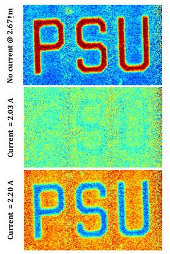
As a proof of concept, the researchers created a .035 inch by .02 inch device and cut the letters PSU into the gold mesh layer so the vanadium dioxide showed through. The researchers photographed the device using an infrared camera at 2.67 microns. Without any current flowing through the device, the PSU stands out as highly reflective. With a current of 2.03 amps, the PSU fades into the background and becomes invisible, while at 2.20 amps, the PSU is clearly visible but the background has become highly reflective.
The response of the vanadium dioxide is tunable by altering the current flowing through the device. According to the researchers, vanadium dioxide can change state very rapidly and it is the device configuration that limits the tuning.
Also working on this project were Liu Liu, recent Ph.D. graduate now at Intel and Theresa S. Mayer, vice president for research and innovation, Virginia Tech.
The National Science Foundation partially funded this work.
Share on:


Testimonial
"Advertising in PCB007 Magazine has been a great way to showcase our bare board testers to the right audience. The I-Connect007 team makes the process smooth and professional. We’re proud to be featured in such a trusted publication."
Klaus Koziol - atgSuggested Items
Beyond Design: Slaying Signal Integrity Villains
09/17/2025 | Barry Olney -- Column: Beyond DesignHigh-speed PCB design is a balancing act, where subtle oversights can develop into major signal integrity nightmares. Some culprits lie dormant during early validation, only to reveal themselves later through workflow disruptions and elusive performance bottlenecks. Take crosstalk, for example. What begins as a stray signal coupling between traces can ripple through the design, ultimately destabilizing the power distribution network. Each of these troublemakers operates with signature tactics, but they also have well-known vulnerabilities.
Driving Innovation: Depth Routing Processes—Achieving Unparalleled Precision in Complex PCBs
09/08/2025 | Kurt Palmer -- Column: Driving InnovationIn PCB manufacturing, the demand for increasingly complex and miniaturized designs continually pushes the boundaries of traditional fabrication methods, including depth routing. Success in these applications demands not only on robust machinery but also sophisticated control functions. PCB manufacturers rely on advanced machine features and process methodologies to meet their precise depth routing goals. Here, I’ll explore some crucial functions that empower manufacturers to master complex depth routing challenges.
Global PCB Connections: Understanding the General Fabrication Process—A Designer’s Hidden Advantage
08/14/2025 | Markus Voeltz -- Column: Global PCB ConnectionsDesigners don’t need to become fabricators, but understanding the basics of PCB fabrication can save you time, money, and frustration. The more you understand what’s happening on the shop floor, the better you’ll be able to prevent downstream issues. As you move into more advanced designs like HDI, flex circuits, stacked vias, and embedded components, this foundational knowledge becomes even more critical. Remember: the fabricator is your partner.
I-Connect007 Editor’s Choice: Five Must-Reads for the Week
08/08/2025 | Andy Shaughnessy, I-Connect007If you’ve been watching the news lately, you might be tempted to opine, “What’s going on here?” In this week’s must-reads, we have a wrap-up of the latest news about U.S. tariffs with Asia, and columnist Tom Yang explains why some PCB fabrication business should remain in China. We also have a piece that examines the unprecedented growth that green manufacturing is expected to see over the next four years.
Driving Innovation: Inner Layer Alignment Methods in PCB Production
08/06/2025 | Kurt Palmer -- Column: Driving InnovationIn PCB manufacturing, precision is a fundamental requirement. Among many complex processes, the accurate registration of inner layers before lamination is one of the most critical. Much like a child's game where rings must be perfectly stacked onto a single pin, PCB manufacturers align multiple conductive and insulating layers to form a cohesive, functional board. This alignment directly affects PCB precision; tighter layer alignment results in smaller "annular rings," superior performance, and higher yields.