-
-
News
News Highlights
- Books
Featured Books
- I-Connect007 Magazine
Latest Issues
Current Issue
Beyond the Rulebook
What happens when the rule book is no longer useful, or worse, was never written in the first place? In today’s fast-moving electronics landscape, we’re increasingly asked to design and build what has no precedent, no proven path, and no tidy checklist to follow. This is where “Design for Invention” begins.
March Madness
From the growing role of AI in design tools to the challenge of managing cumulative tolerances, these articles in this issue examine the technical details, design choices, and manufacturing considerations that determine whether a board works as intended.
Looking Forward to APEX EXPO 2026
I-Connect007 Magazine previews APEX EXPO 2026, covering everything from the show floor to the technical conference. For PCB designers, we move past the dreaded auto-router and spotlight AI design tools that actually matter.
- Articles
- Columns
- Links
- Media kit
||| MENU - I-Connect007 Magazine
LPKF Announces First Sales of the New ProtoLaser R in Asia
December 21, 2016 | LPKFEstimated reading time: 1 minute
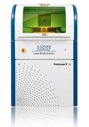
For the past 40 years, LPKF has been the global market leader in the field of systems for manufacturing PCBs in development laboratories. And now the Garbsen-based company is rounding off the high-end of this segment with a world first: the ProtoLaser R is the first system optimized for the use in development departments using an ultrashort picosecond pulse laser, allowing it to work on highly sensitive materials thanks to the lack of heat input. With its compactness and price, the LPKF ProtoLaser R is currently one of a kind on the market.
Research activities as well as process and product development require flexible and high-precision tools. The requirements of developers are becoming increasingly stringent, primarily due to the trend toward ever more sophisticated materials and even smaller dimensions. With the ProtoLaser R, LPKF is opening up new opportunities for laboratory-based experimentation with completely new materials in the micro and nano range.
LPKF sees the sale of the first two systems to customers in Asia as a vote of confidence in the future of the DevelopmentQuipment (DQ) segment. “With this product, we have developed a new laboratory laser system that is currently unrivaled,” says Dr. Ingo Bretthauer, CEO of LPKF AG. Our technology sees us for the first time entering the world of research, which will be of strategic importance to future production.”
About LPKF
Established in 1976, LPKF Laser & Electronics manufactures milling machines and laser systems used in circuit board and microelectronics fabrication, medical technology, the automotive sector, and the production of solar cells. LPKF’s worldwide headquarters is located in Hannover, Germany and its North American headquarters resides near Portland, Ore.
Testimonial
"Your magazines are a great platform for people to exchange knowledge. Thank you for the work that you do."
Simon Khesin - Schmoll MaschinenSuggested Items
Advanced Materials Roundtable
04/23/2026 | I-Connect007 Editorial TeamDriven largely by the need for advanced chip technology for super compute ability and AI applications, low Dk, low-loss resin systems, and heavy copper laminate are attracting significant attention and global resources. There are numerous unavoidable challenges in this market that will impact manufacturers and the supply chain, and they may be hitting critical mass sooner than OEMs and fabricators think. In this roundtable discussion, moderator Marcy LaRont speaks with topic experts: Mark Goodwin, John Fix, and Ed Kelly.
Silicon Box Joins imec Automotive Chiplet Program to Strengthen Next-Gen Vehicle Supply Chains
04/22/2026 | PRNewswireSilicon Box, an industry leader in advanced semiconductor packaging solutions, announced that it has formally joined imec's Automotive Chiplet Program (ACP), a collaborative research initiative aimed at accelerating chiplet technology adoption required to drive the development of next-generation vehicles.
Mitate Zepto Technica Joins JST Edge AI Semiconductor R&D Program as Implementation Partner
04/22/2026 | PRNewswireMitate Zepto Technica, Inc., based in Tokyo's Shibuya district, announced on April 20 that it has joined the national research initiative "Next-Generation Edge AI Semiconductor Research and Development Program" promoted by the Japan Science and Technology Agency (JST).
Wearable Technology Market Expected to Reach $183.2 Billion by 2031, Growing at a CAGR of 12.75%
04/22/2026 | PRNewswireAccording to the report, the global wearable technology market size was valued at USD 54.8 billion in 2020 and is projected to reach USD 183.2 billion by 2031, registering a CAGR of 12.75% from 2022 to 2031.
Camtek Acquires Visual Layer to Strengthen Visual AI Capabilities in Inspection and Metrology
04/21/2026 | CamtekCamtek Ltd., a leading developer and manufacturer of inspection and metrology equipment for the semiconductor industry, announced that it has signed a definitive agreement to acquire Visual Layer, a Tel Aviv-based AI company specializing in visual analytics.