


 Punching Out: M&A Deals in North American PCB and EMS Sectors for the First Half of 2026
 Trouble in Your Tank: At 40 GHz, Everything Matters, Part 2
 It’s Only Common Sense: Stop Watching the Headlines and Start Watching the Opportunity


Sandia National Laboratories researchers have shown it’s possible to make transistors and diodes from advanced semiconductor materials that could perform much better than silicon, the workhorse of the modern electronics world.
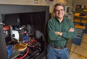
Sandia National Laboratories electrical engineer Bob Kaplar heads a project studying ultrawide bandgap semiconductor materials. The project is answering such questions as how materials behave and how to work with them, steps toward improving everything from consumer electronics to power grids. (Photo by Randy Montoya)
The breakthrough work takes a step toward more compact and efficient power electronics, which in turn could improve everything from consumer electronics to electrical grids. Power electronics are vital for electrical systems because they transfer power from its source to the load, or user, by converting voltages, currents and frequencies. Sandia’s research was published this summer in Applied Physics Letters and Electronics Letters and presented at conferences.
“The goal is to be able to shrink power supplies, power conversion systems,” said electrical engineer Bob Kaplar, who leads a Laboratory Directed Research and Development project studying ultrawide bandgap (UWBG) semiconductor materials. The project explores ways to grow those materials with fewer defects and create different device designs that exploit the properties of these new materials that have significant advantages over silicon.
The project is laying the scientific groundwork for the new UWBG research area, answering such questions as how the materials behave and how to work with them. It also will aid Sandia’s broader work through developments, such as compact power conversion by using better semiconductor devices. “Understanding the science helps lead toward that second goal,” Kaplar said.
Bandgap is a fundamental materials property that helps determine electrical conductivity and ultimately transistor performance. Wide bandgap (WBG) materials allow devices to operate at higher voltages, frequencies and temperatures, and are starting to have impact on power conversion systems. Emerging ultrawide bandgap materials are even more attractive because they could allow further scaling to devices that operate at even higher voltages, frequencies and temperatures. When made into transistors, the materials have the potential to vastly improve the performance and efficiency of electrical power grids, electric vehicles, computer power supplies and motors for such things as heating, ventilation and air conditioning (HVAC) systems. Faster switching also could lead to smaller capacitors and associated circuit components, miniaturizing the entire power system.
Work demonstrates highest-bandgap transistor
Sandia researchers demonstrated the highest-bandgap transistor ever, a High Electron Mobility Transistor, and published those results in the July 18 edition of Applied Physics Letters. Sandia published papers in June and July in Electronics Letters analyzing the performance of diodes made from gallium nitride (GaN) and aluminum gallium nitride (AlGaN).
“All three of these papers represent progress on the road to more compact and higher-efficiency power converters,” Kaplar said. “They are also very exciting developments in semiconductor materials and device physics in their own right.”
However, he cautioned that the work doesn’t mean UWBG devices are ready for the marketplace.
“There are a lot more improvements that need to be made to the transistor,” he said. “The same with the diodes. There’s a lot more optimization that needs to be done, a lot we don’t understand about their behavior.”
Researchers at Sandia and elsewhere have studied WBG materials, such as silicon carbide (SiC) and GaN, for about two decades. In recent years, Sandia also has looked at next-generation UWBG materials, such as AlGaN. In fact, Sandia coined the term ultrawide bandgap, which has caught on throughout the research community, Kaplar said.
Researchers studying best way to grow new materials
One critical piece of the puzzle is figuring out the best way to grow new semiconductor materials. Researchers also must understand defects in the materials, how to process materials into working devices and find ways to improve passive elements, such as magnetic inductors.
Semiconductor materials are characterized by their efficiency and effectiveness, so it’s easy to assume you could make a power supply 10 times smaller if one material is 10 times better than another. But it’s not that simple. “It depends on other components in the power converter. There’s magnetics, there’s capacitors,” Kaplar said. “We’re starting to look at what is a more realistic scaling.”
He and his colleagues collaborate with Sandia experts in other fields to understand the relationship of semiconductors to other components in a system. “The semiconductor enables the system, but if you have something else that’s limiting it, then you can’t reach the semiconductor’s full potential for shrinking the size of power conversion,” Kaplar said.
Better semiconductor materials would mean higher absolute voltages for such uses as distributing power grid energy. Right now that’s done by stacking devices in series to reach a desired combined voltage. Since UWBG materials have higher voltages than more traditional materials, far fewer devices would be needed in the stack. Kaplar said UWBG materials also could be useful at extreme temperatures or radiation environments — applications of interest for nuclear weapons or satellites.
Because of the potential impact on so much of Sandia’s work, Kaplar expects UWBG research to continue after the current project ends next September. “We lay the foundation and then we want it to continue to advance, both the science and the eventual applications.”
Authors of the Applied Physics Letters paper are Albert Baca, Andrew Armstrong, Andrew Allerman, Erica Douglas, Carlos Sanchez, Michael King, Michael Coltrin, Torben Fortune and Kaplar. Team members also presented the results at the Device Research Conference at the University of Delaware in June and the Lester Eastman Conference on High Performance Devices at Lehigh University in August.


