


 It’s Only Common Sense: Create Passion That Customers Feel
 Punching Out: How to Stay Focused in Business and M&A


The “internet of things” is the idea that vehicles, appliances, civil structures, manufacturing equipment, and even livestock will soon have sensors that report information directly to networked servers, aiding with maintenance and the coordination of tasks.
Those sensors will have to operate at very low powers, in order to extend battery life for months or make do with energy harvested from the environment. But that means that they’ll need to draw a wide range of electrical currents. A sensor might, for instance, wake up every so often, take a measurement, and perform a small calculation to see whether that measurement crosses some threshold. Those operations require relatively little current, but occasionally, the sensor might need to transmit an alert to a distant radio receiver. That requires much larger currents.
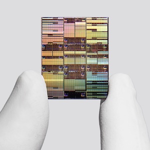
Generally, power converters, which take an input voltage and convert it to a steady output voltage, are efficient only within a narrow range of currents. But at the International Solid-State Circuits Conference last week, researchers from MIT’s Microsystems Technologies Laboratories (MTL) presented a new power converter that maintains its efficiency at currents ranging from 500 picoamps to 1 milliamp, a span that encompasses a 2,000,000-fold increase.
“Typically, converters have a quiescent power, which is the power that they consume even when they’re not providing any current to the load,” says Arun Paidimarri, who was a postdoc at MTL when the work was done and is now at IBM Research. “So, for example, if the quiescent power is a microamp, then even if the load pulls only a nanoamp, it’s still going to consume a microamp of current. My converter is something that can maintain efficiency over a wide range of currents.”
Paidimarri, who also earned doctoral and master’s degrees from MIT, is first author on the conference paper. He’s joined by his thesis advisor, Anantha Chandrakasan, the Vannevar Bush Professor of Electrical Engineering and Computer Science at MIT.
Packet perspective
The researchers’ converter is a step-down converter, meaning that its output voltage is lower than its input voltage. In particular, it takes input voltages ranging from 1.2 to 3.3 volts and reduces them to between 0.7 and 0.9 volts.
“In the low-power regime, the way these power converters work, it’s not based on a continuous flow of energy,” Paidimarri says. “It’s based on these packets of energy. You have these switches, and an inductor, and a capacitor in the power converter, and you basically turn on and off these switches.”
The control circuitry for the switches includes a circuit that measures the output voltage of the converter. If the output voltage is below some threshold — in this case, 0.9 volts — the controllers throw a switch and release a packet of energy. Then they perform another measurement and, if necessary, release another packet.
If no device is drawing current from the converter, or if the current is going only to a simple, local circuit, the controllers might release between 1 and a couple hundred packets per second. But if the converter is feeding power to a radio, it might need to release a million packets a second.
To accommodate that range of outputs, a typical converter — even a low-power one — will simply perform 1 million voltage measurements a second; on that basis, it will release anywhere from 1 to 1 million packets. Each measurement consumes energy, but for most existing applications, the power drain is negligible. For the internet of things, however, it’s intolerable.
Clocking down
Paidimarri and Chandrakasan’s converter thus features a variable clock, which can run the switch controllers at a wide range of rates. That, however, requires more complex control circuits. The circuit that monitors the converter’s output voltage, for instance, contains an element called a voltage divider, which siphons off a little current from the output for measurement. In a typical converter, the voltage divider is just another element in the circuit path; it is, in effect, always on.
But siphoning current lowers the converter’s efficiency, so in the MIT researchers’ chip, the divider is surrounded by a block of additional circuit elements, which grant access to the divider only for the fraction of a second that a measurement requires. The result is a 50 percent reduction in quiescent power over even the best previously reported experimental low-power, step-down converter and a tenfold expansion of the current-handling range.
“This opens up exciting new opportunities to operate these circuits from new types of energy-harvesting sources, such as body-powered electronics,” Chandrakasan says.
“This work pushes the boundaries of the state of the art in low-power DC-DC converters, how low you can go in terms of the quiescent current, and the efficiencies that you can achieve at these low current levels,” says Yogesh Ramadass, the director of power management research at Texas Instruments’ Kilby Labs. “You don’t want your converter to burn up more than what is being delivered, so it’s essential for the converter to have a very low quiescent power state.”
The work was funded by Shell and Texas Instruments, and the prototype chips were built by the Taiwan Semiconductor Manufacturing Corporation, through its University Shuttle Program.


