-
- News
- Books
Featured Books
- pcb007 Magazine
Latest Issues
Current IssueIn Pursuit of Perfection: Defect Reduction
For bare PCB board fabrication, defect reduction is a critical aspect of a company's bottom line profitability. In this issue, we examine how imaging, etching, and plating processes can provide information and insight into reducing defects and increasing yields.
Voices of the Industry
We take the pulse of the PCB industry by sharing insights from leading fabricators and suppliers in this month's issue. We've gathered their thoughts on the new U.S. administration, spending, the war in Ukraine, and their most pressing needs. It’s an eye-opening and enlightening look behind the curtain.
The Essential Guide to Surface Finishes
We go back to basics this month with a recount of a little history, and look forward to addressing the many challenges that high density, high frequency, adhesion, SI, and corrosion concerns for harsh environments bring to the fore. We compare and contrast surface finishes by type and application, take a hard look at the many iterations of gold plating, and address palladium as a surface finish.
- Articles
- Columns
Search Console
- Links
- Media kit
||| MENU - pcb007 Magazine
SelectConnect Technologies Publishes White Paper on Laser Direct Structuring
April 5, 2017 | SelectConnect TechnologiesEstimated reading time: 1 minute

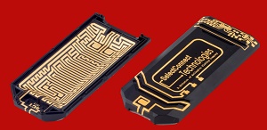
SelectConnect Technologies has published the white paper, “Trace Width and Space Limitations for Laser Direct Structuring.” The white paper details a study that was conducted to determine how close laser direct structuring (LDS) traces can be created and metallized without inducing over plating or bridging on PET/PBT material.
A geometric pattern with varying trace widths and spacing distances were structured onto plaques made from the three different materials. The plaques were subsequently plated with copper, nickel, and immersion gold and examined for signs of over plating. Trace widths and spacing were measured using video microscopy equipment.
Laser direct structuring (LDS) is the first step of a manufacturing process that creates circuit traces on three-dimensional molded thermoplastic components. Currently the leading technology for producing cell phone antennas, LDS has also been widely employed to manufacture a range of components for use in medical devices, security shields, automotive sensors, and GPS antennas-- anywhere product miniaturization requires embedding circuits onto a molded component of a device.
About SelectConnect Technologies
SelectConnect Technologies specializes in the production of three-dimensional molded interconnect devices (3D-MID), offering both laser direct structuring (LDS) and 2-shot injection capabilities. Working with LPKF since 2010, the company has produced thousands of laser direct structured components for a wide range of applications. With expertise in electroless metallization, SelectConnect also produces molded interconnect device plating to construct circuitry with the comparable function and performance of a printed circuit board.
To read and download the white paper, please click here or email solutions@selectconnettech.com.
Suggested Items
Preventing Surface Prep Defects and Ensuring Reliability
06/10/2025 | Marcy LaRont, PCB007 MagazineIn printed circuit board (PCB) fabrication, surface preparation is a critical process that ensures strong adhesion, reliable plating, and long-term product performance. Without proper surface treatment, manufacturers may encounter defects such as delamination, poor solder mask adhesion, and plating failures. This article examines key surface preparation techniques, common defects resulting from improper processes, and real-world case studies that illustrate best practices.
RF PCB Design Tips and Tricks
05/08/2025 | Cherie Litson, EPTAC MIT CID/CID+There are many great books, videos, and information online about designing PCBs for RF circuits. A few of my favorite RF sources are Hans Rosenberg, Stephen Chavez, and Rick Hartley, but there are many more. These PCB design engineers have a very good perspective on what it takes to take an RF design from schematic concept to PCB layout.
Trouble in Your Tank: Causes of Plating Voids, Pre-electroless Copper
05/09/2025 | Michael Carano -- Column: Trouble in Your TankIn the business of printed circuit fabrication, yield-reducing and costly defects can easily catch even the most seasoned engineers and production personnel off guard. In this month’s column, I’ll investigate copper plating voids with their genesis in the pre-plating process steps.
Elephantech: For a Greener Tomorrow
04/16/2025 | Marcy LaRont, PCB007 MagazineNobuhiko Okamoto is the global sales and marketing manager for Elephantech Inc., a Japanese startup with a vision to make electronics more sustainable. The company is developing a metal inkjet technology that can print directly on the substrate and then give it a copper thickness by plating. In this interview, he discusses this novel technology's environmental advantages, as well as its potential benefits for the PCB manufacturing and semiconductor packaging segments.
Trouble in Your Tank: Organic Addition Agents in Electrolytic Copper Plating
04/15/2025 | Michael Carano -- Column: Trouble in Your TankThere are numerous factors at play in the science of electroplating or, as most often called, electrolytic plating. One critical element is the use of organic addition agents and their role in copper plating. The function and use of these chemical compounds will be explored in more detail.