


 American Made Advocacy: Five Years of Educating, Advocating, and Influencing Legislation and Policy
 Defense Speak Interpreted: Understanding What the Department of Defense Is, and Isn’t
 The Right Approach: The End of an Era—DoD Proposes MIL-PRF-31032 Cancellation


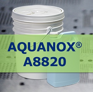
KYZEN today announced plans to exhibit in the tabletop portion of the Contamination, Cleaning & Coating Conference, scheduled to take place May 22-24, 2017 in Amsterdam. The event is co-organized by SMTA and SMART Group. The KYZEN team will showcase its AQUANOX A8820 Advanced Aqueous Stencil Cleaner, designed from the ground up for the tough challenges of cleaning no-clean, lead-free residue from small, 1005 apertures while being compatible with modern nano-coatings as well as with all of the modern offline cleaning equipment that is popular in the industry. A8820 is a quick drying product that also is rapidly rinsed if water rinsing is preferred.
AQUANOX A8820 is an engineered Micro Cell Technology (MCT™) cleaning fluid designed to remove wet solder paste and uncured chip bonder adhesive from stencils used in surface mount printing processes. It effectively removes common solder pastes and fluxes, and demonstrates a favorable compatibility profile with stencil cleaning systems.
A8820 works well with spray-in-air and select ultrasonic cleaning machines, and is effective on uncured adhesives. Additionally, the no-foaming property of A8820 is compatible with all materials commonly used in electronic assembly manufacturing and cleaning processes.
AQUANOX A8820 is available in in one, five, and 55 gallon containers.
KYZEN is a worldwide leading supplier of precision cleaning chemistries to the electronics, metal finishing, medical, semiconductor, and optical industries. The company connects leading science with care to create the most effective cleaning solutions for each customer’s unique manufacturing process or problem.
About KYZEN
KYZEN is a global leader in providing environmentally responsible, RoHS compliant precision cleaning chemistries for industries ranging from electronics and advanced packaging to metal finishing and aerospace applications. Since its founding in 1990, KYZEN’s innovative cleaning technologies, scientific expertise and customer support have been repeatedly recognized with the industry’s most prestigious awards. For more information, click here.


