


 The Marketing Minute: Cracking the Code of Technical Marketing
 Trouble in Your Tank: Implementing Direct Metallization in Advanced Substrate Packaging


Graphene and Quantum Dots Put in Motion a CMOS-Integrated Camera That Can See the Invisible
May 30, 2017 | ICFOEstimated reading time: 2 minutes
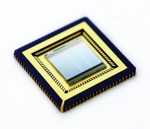
ICFO develops the first graphene-quantum dot based CMOS integrated camera, capable of imaging visible and infrared light at the same time.Over the past 40 years, microelectronics has advanced by leaps and bounds thanks to silicon and CMOS (Complementary metal-oxide semiconductors) technology, making possible computing, smartphones, compact and low-cost digital cameras, as well as most of the electronic gadgets we rely on today. However, the diversification of this platform into applications other than microcircuits and visible light cameras has been impeded by the difficulty to combine semiconductors other than silicon with CMOS.
This obstacle has now been overcome. ICFO researchers have shown for the first time the monolithic integration of a CMOS integrated circuit with graphene, resulting in a high-resolution image sensor consisting of hundreds of thousands of photodetectors based on graphene and quantum dots (QD). They operated it as a digital camera that is highly sensitive to UV, visible and infrared light at the same time. This has never been achieved before with existing imaging sensors. In general, this demonstration of monolithic integration of graphene with CMOS enables a wide range of optoelectronic applications, such as low-power optical data communications and compact and ultra sensitive sensing systems.
The study was published in Nature Photonics, and highlighted on the front cover image. The work was carried out by ICFO researchers Stijn Goossens, Gabriele Navickaite, Carles Monasterio, Schuchi Gupta, Juan Jose Piqueras, Raul Perez, Gregory Burwell, Ivan Nitkitsky, Tania Lasanta, Teresa Galan, Eric Puma, and led by ICREA Professors Frank Koppens and Gerasimos Konstantatos, in collaboration with the company Graphenea. The graphene-QD image sensor was fabricated by taking PbS colloidal quantum dots, depositing them onto the CVD graphene and subsequently depositing this hybrid system onto a CMOS wafer with image sensor dies and a read-out circuit. As Stijn Goossens comments, “No complex material processing or growth processes were required to achieve this graphene-quantum dot CMOS image sensor. It proved easy and cheap to fabricate at room temperature and under ambient conditions, which signifies a considerable decrease in production costs. Even more, because of its properties, it can be easily integrated on flexible substrates as well as CMOS-type integrated circuits.”
As ICREA Prof. at ICFO Gerasimos Konstantatos, expert in quantum dot-graphene research comments, “we engineered the QDs to extend to the short infrared range of the spectrum (1100-1900nm), to a point where we were able to demonstrate and detect the night glow of the atmosphere on a dark and clear sky enabling passive night vision. This work shows that this class of phototransistors may be the way to go for high sensitivity, low-cost, infrared image sensors operating at room temperature addressing the huge infrared market that is currently thirsty for cheap technologies”.
“The development of this monolithic CMOS-based image sensor represents a milestone for low-cost, high-resolution broadband and hyperspectral imaging systems” ICREA Prof. at ICFO Frank Koppens highlights. He assures that “in general, graphene-CMOS technology will enable a vast amount of applications, that range from safety, security, low cost pocket and smartphone cameras, fire control systems, passive night vision and night surveillance cameras, automotive sensor systems, medical imaging applications, food and pharmaceutical inspection to environmental monitoring, to name a few”.
This project is currently incubating in ICFO’s Launchpad. The team is working with the institute’s tech transfer professionals to bring this breakthrough along with its full patent portfolio of imaging and sensing technologies to the market.
This research has been partially supported by the European Graphene Flagship, the European Research Council, the Government of Catalonia, Fundació Cellex and the Severo Ochoa Excellence program of the Government of Spain.
Share on:


Testimonial
"We’re proud to call I-Connect007 a trusted partner. Their innovative approach and industry insight made our podcast collaboration a success by connecting us with the right audience and delivering real results."
Julia McCaffrey - NCAB GroupSuggested Items
I-Connect007 Editor’s Choice: Five Must-Reads for the Week
08/15/2025 | Marcy LaRont, I-Connect007In our industry, my top reads include Prashant Patel’s overview and argument for reshoring, which I found to be a great general overview and breakdown. In further support of the onshoring/reshoring message, I’m highlighting Nolan Johnson’s interview on the survey and report by the Reshoring Initiative. Check out my interview with USPAE’s Jim Will on the state of the flat panel display (FPD) industry and the risks associated with it for U.S. defense and critical infrastructure products.
Global Electronics Industry Remains Under Pressure from Rising Costs
08/04/2025 | Global Electronics AssociationThe global electronics manufacturing supply chain remains under pressure from rising costs, with 61% of firms reporting higher material costs and 54% noting increased labor expenses. according to the Global Electronics Association’s Sentiment of the Global Electronics Manufacturing Supply Chain Report.
Statement from the Global Electronics Association on the July 2025 Tariff on Copper Foil and Electronics-Grade Copper Inputs
07/31/2025 | Global Electronics AssociationWe are disappointed by today’s decision to impose a 50% tariff on imported copper foil and other essential materials critical to electronics manufacturing in the United States.
Direct Metallization: A Sustainable Shift in PCB Fabrication
07/31/2025 | Jim Watkowski, Harry Yang, and Mark Edwards, MacDermid Alpha Electronics SolutionsThe global electronics industry is undergoing a significant transformation, driven by the need for more resilient supply chains and environmentally sustainable manufacturing practices. Printed circuit boards (PCBs), the backbone of interconnection for electronic devices, are at the center of this shift. Traditionally, PCB fabrication has relied heavily on electroless copper, a process that, while effective, is resource-intensive and environmentally hazardous. In response, many manufacturers are turning to direct metallization technologies as a cleaner, more efficient alternative.
Considering the Future of Impending Copper Tariffs
07/30/2025 | I-Connect007 Editorial TeamThe Global Electronics Association is alerting industry members that a potential 50% tariff on copper could hit U.S. electronics manufacturers where it hurts.