


 Beyond the Board: What Companies Need to Know Before Entering the MilAero PCB Market
 Defense Speak Interpreted: If CHIPS Cuts Back, What Happens to Electronics Packaging Funds?
 American Made Advocacy: Where’s the Budget for a Modern Military Run on Microelectronics?


Researchers Discovered New Method for Improving Perovskite Solar Cell Performance
June 22, 2017 | Aalto UniversityEstimated reading time: 2 minutes
The Aalto-developed treatment builds on previous breakthroughs improving the efficiency and longevity of perovskite solar cells using established printing methods (carbon back contact based perovskite solar cells or CPSCs). These findings make it possible to further enhance the efficiency of these types of solar cells.
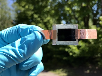
A humidity assisted and thermal treated (HTE) carbon-based printed perovskite solar cell. Photo: Ghufran Hashmi.
Perovskite solar cells are solar cells where the light harvesting layer consists of lead halide with perovskite crystal structure. Globally, perovskite cells are studied intensively since they might prove to be an alternative to silicon cells that require a lot of energy in the manufacturing process.
In the new method, the perovskite solar cells were exposed to 40-degrees in a chamber where humidity was kept in the level of 70% (±5%). This kind of environment normally degrades the properties of perovskite solar cells. In this case, the treatment led to surprising growth of the perovskite crystals, which naturally absorb sunlight and generate electricity.
“The photovoltaic performance was significantly enhanced, and the overall efficiency increased almost 45%,” says Dr Ghufran Hashmi, an Academy of Finland postdoctoral researcher.
“Ghufran Hashmi was interested in possible changes in the atomic structure of the perovskite solar cells. With the state-of-the-art X-ray diffractometer of the Nanomicroscopy Center at Aalto, we were able to monitor the crystallite structure of the perovskite layer before and after the treatment,” says Dr Ulla Vainio, a staff scientist in the Department of Applied Physics, who assisted Hashmi with collecting experimental data.
The team did not stop there, but examined the perovskites using a scanning electron microscopy (SEM). “The SEM images supported the previous observations obtained from the X-ray diffraction method analysis, which endorsed the gradual crystal growth over the period of exposure,” reports Dr Teemu Sarikka, a staff scientist in the Department of Mechanical Engineering.
The task of physics doctoral student Teemu Myllymäki was to check if any chemical changes occurred in the perovskite crystal structure induced by the moisture generated by the thermo-humid environment. In his research, Myllymäki utilized Fourier transform infrared spectroscopy (FTIR). “The comparison between the fresh and exposed solar cells revealed almost no change in the chemical structure of the perovskite light absorbing layer, which endorses the successful implementation of this new treatment method,” he reports.
Solar cells are part of the rapidly expanding area of next-generation, low-cost photovoltaic systems. The team at Aalto benefited from working with collaborators in Switzerland, the Solaronix company and the Swiss Federal Institute of Technology (EPFL) in Lausanne. “Solaronix provided the samples and EPFL researcher Dr Ibrahim Dar helped us in key processes that are critically required for the successful commercialization of this low cost solar cell technology,” says Dr Hashmi.
The team from Aalto University involved in this research work with an HTE treated carbon based printed perovskite solar cell. From left to right: Teemu Myllymäki, Ghufran Hashmi, Ulla Vainio, Teemu Sarikka. Photo: Nonappa.
Share on:


Testimonial
"We’re proud to call I-Connect007 a trusted partner. Their innovative approach and industry insight made our podcast collaboration a success by connecting us with the right audience and delivering real results."
Julia McCaffrey - NCAB GroupSuggested Items
Beyond Design: Slaying Signal Integrity Villains
09/17/2025 | Barry Olney -- Column: Beyond DesignHigh-speed PCB design is a balancing act, where subtle oversights can develop into major signal integrity nightmares. Some culprits lie dormant during early validation, only to reveal themselves later through workflow disruptions and elusive performance bottlenecks. Take crosstalk, for example. What begins as a stray signal coupling between traces can ripple through the design, ultimately destabilizing the power distribution network. Each of these troublemakers operates with signature tactics, but they also have well-known vulnerabilities.
Driving Innovation: Depth Routing Processes—Achieving Unparalleled Precision in Complex PCBs
09/08/2025 | Kurt Palmer -- Column: Driving InnovationIn PCB manufacturing, the demand for increasingly complex and miniaturized designs continually pushes the boundaries of traditional fabrication methods, including depth routing. Success in these applications demands not only on robust machinery but also sophisticated control functions. PCB manufacturers rely on advanced machine features and process methodologies to meet their precise depth routing goals. Here, I’ll explore some crucial functions that empower manufacturers to master complex depth routing challenges.
Global PCB Connections: Understanding the General Fabrication Process—A Designer’s Hidden Advantage
08/14/2025 | Markus Voeltz -- Column: Global PCB ConnectionsDesigners don’t need to become fabricators, but understanding the basics of PCB fabrication can save you time, money, and frustration. The more you understand what’s happening on the shop floor, the better you’ll be able to prevent downstream issues. As you move into more advanced designs like HDI, flex circuits, stacked vias, and embedded components, this foundational knowledge becomes even more critical. Remember: the fabricator is your partner.
I-Connect007 Editor’s Choice: Five Must-Reads for the Week
08/08/2025 | Andy Shaughnessy, I-Connect007If you’ve been watching the news lately, you might be tempted to opine, “What’s going on here?” In this week’s must-reads, we have a wrap-up of the latest news about U.S. tariffs with Asia, and columnist Tom Yang explains why some PCB fabrication business should remain in China. We also have a piece that examines the unprecedented growth that green manufacturing is expected to see over the next four years.
Driving Innovation: Inner Layer Alignment Methods in PCB Production
08/06/2025 | Kurt Palmer -- Column: Driving InnovationIn PCB manufacturing, precision is a fundamental requirement. Among many complex processes, the accurate registration of inner layers before lamination is one of the most critical. Much like a child's game where rings must be perfectly stacked onto a single pin, PCB manufacturers align multiple conductive and insulating layers to form a cohesive, functional board. This alignment directly affects PCB precision; tighter layer alignment results in smaller "annular rings," superior performance, and higher yields.