











-
- News
- Books
Featured Books
- smt007 Magazine
Latest Issues
Current Issue
Spotlight on North America
A North America spotlight exploring tariffs, reshoring, AI demand, and supply chain challenges. Plus, insights on cybersecurity, workforce development, and the evolving role of U.S. electronics manufacturing.
Wire Harness Solutions
Explore what’s shaping wire harness manufacturing, and how new solutions are helping companies streamline operations and better support EMS providers. Take a closer look at what’s driving the shift.
Spotlight on Europe
As Europe’s defense priorities grow and supply chains are reassessed, industry and policymakers are pushing to rebuild regional capability. This issue explores how Europe is reshaping its electronics ecosystem for a more resilient future.
- Articles
- Columns
- Links
- Media kit
||| MENU - smt007 Magazine
Akrometrix Launches New Warpage Metrology System
June 29, 2017 | Akrometrix LLCEstimated reading time: 1 minute
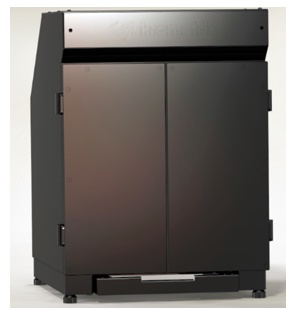
Akrometrix, LLC, the leading provider of thermal warpage and strain metrology equipment to both the front- and back-end semiconductor and electronics industries, is pleased to announce that it has launched its newest warpage metrology system – the Tabletop Shadow Moiré (TTSM) system.
“Over the years, many of our customers who are using our systems for thermal warpage metrology have stated a need for an ultra-fast, highly accurate room temperature warpage metrology system,” stated Mayson Brooks, Akrometrix President. “Additionally, they wanted a system that was small enough for a tabletop operation and that would allow them to utilize all the software features of our thermal warpage systems, only at room temperature.”
The TTSM meets this demand – enabling customers to measure warpage of substrates up to 300mm x 310 mm (a 300mm wafer or two JEDEC trays) with the entire measurement taking less than two seconds. Whether individual parts or a JEDEC tray of multiple parts, the TTSM provides an ultra-fast and highly accurate measurement at room temperature that is suited for tabletop use.
About Akrometrix LLC
Akrometrix is the leader in thermal warpage and strain metrology for the front-end/back-end wafer, back-end packaging/assembly, panel and the PCB/component markets. The company provides both capital equipment and test services to measure warpage and strain in temperatures from -50°C to 300°C on virtually any substrate up to 600mm x 600mm, regardless of shape. Located in Atlanta, Georgia, Akrometrix has been serving customers worldwide for more than 20 years based on technology developed at Georgia Tech. For more information click here.
Testimonial
"The I-Connect007 team is outstanding—kind, responsive, and a true marketing partner. Their design team created fresh, eye-catching ads, and their editorial support polished our content to let our brand shine. Thank you all! "
Sweeney Ng - CEE PCBSuggested Items
Kymeta Joins Red Cat Initiative for Maritime Connectivity
05/15/2026 | Globe NewswireRed Cat Holdings, Inc. , a U.S.-based provider of advanced all-domain drone and robotic solutions for defense and national security, announced that Kymeta, a world-leading flat-panel satellite terminal manufacturer, has joined the Red Cat Futures Initiative, the company’s industry-wide consortium accelerating advanced autonomous systems for modern warfare.
SPARK Microsystems Selected for CAD $1M in Government of Canada-backed FABrIC Funding
05/14/2026 | BUSINESS WIRESPARK Microsystems, a Canadian fabless semiconductor company specializing in next-generation short-range wireless communications, has been selected by FABrIC as a CAD $1 million grant recipient funded by the Government of Canada.
System Architecture Beyond the Die With Advanced Packaging as the Scaling Factor
05/14/2026 | Chetan Arvind Patil, Marvell TechnologyIn conventional monolithic semiconductor design, system integration was achieved within a single die and constrained by reticle limits. Compute cores, cache, memory controllers, and input output (I/O) interfaces were all co-optimized on a single process node, with performance closely tied to transistor density and on-die interconnect efficiency. This monolithic system-on-chip (SoC) approach enabled low-latency communication and relatively straightforward power delivery. However, as design for compute-intensive SoCs approaches reticle limits and advanced-node costs increase, the ability to continue scaling within a single die begins to diminish.
Rethinking Reinforcement Materials for Advanced Packaging
05/14/2026 | Ivana Ivanovic, Flexiramics B.V.Materials that once quietly supported the industry are now becoming limiting factors. The electronics industry is experiencing unprecedented pressure as RF systems push into mmWave frequencies, high-speed digital architectures advance into their next performance generation, and power densities climb across automotive, telecom, aerospace, and computing. Reinforcement materials, long treated as a background detail in laminate design, are suddenly at the centre of performance, reliability, and supply‑chain discussions.
Below the Surface: Active Component and Module Submounts—The Architecture Behind Performance
05/14/2026 | Chandra Gupta -- Column: Below the SurfaceIf you were to peel back the layers of a modern electronic system, such as a satellite transceiver, a LiDAR module, or a 5G base station, you would not immediately notice a specific component doing some of the most important work. It doesn’t amplify signals, emit light, or process data, yet without it, none of those functions would be stable, reliable, or scalable. That component is the active device submount.