


 Knocking Down the Bone Pile: The Business Case for Component Reclamation
 Global Sourcing Spotlight: The Hidden Power of the Rep Network
 Smart Automation: When Traditional Depaneling Methods Reach Their Limits


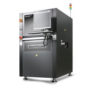
Koh Young Technology will launch its new Meister Series at SEMICON West, which will be held July 11–13 at the Moscone Center in San Francisco, California.
The series, which includes Meister-SPi (solder paste inspection) and Meister-MCi (mounted chip inspection), will be on display with the new theme “True 3D now powered by Intelligent Platform for Smart Factory” at Koh Young’s booth (5150).
Koh Young’s Meister, as the name implies, has the most optimized 3D inspection solutions for advanced IC packaging. For example, it can measure volume, area, height, and diameter of virtually any packaging like SiP, 2.5D, 3D WLP, WLCSP, and FOWLP, among others. Also, Koh Young’s powerful SPC@KSMART allows tracking a wide range of defects from insufficient/excess solder, to bridge, XY position, abnormal shape, and applying changes to inspection programs in real-time.
Another distinguishing feature of Meister series is its simple inspection setting. Due to its user-friendly inspection setting software, no fine-tuning or base reference teaching is required.
The Meister-SPi combines Koh Young’s innovative vision algorithms with advanced high-resolution optics for the semiconductor industries. This innovative SPi system will be configured with high resolution 12MP 5µm optics and high-speed camera, offering best-in-class inspection capability for mass production. With precise resolution, Meister-SPi enables down to 10µm thin solder inspection.
The Meister-MCi, the 3D Automated Optical (AOI) solutions for semiconductor business, helps enhancing the manufacturing yields and product reliability with high WPH (wafer per hour). With advanced image processing at mass production line, it allows accurate measurement of high height object.
“Having a strong reputation in US market, Koh Young has been helping worldwide 2,400 customers to realize agile manufacturing innovation,” stated Jay Park, Head of Semicon Business Division at Koh Young Technology. “We are excited to show our latest innovations to visitors in upcoming SEMICON West.”
About Koh Young Technology Inc.
Koh Young Technology, a leading provider of Solder Paste Inspection (SPI) and Automated Optical Inspection (AOI) systems, specializes in the design and manufacturing of 3D measurement and inspection equipment for the global circuit board assembly and semiconductor markets. Direct sales and support centers are in the United States, Germany, Japan, Singapore, China and Korea. For more information about the company, visit www.kohyoung.com.


