


 Global Sourcing Spotlight: Making Global Sourcing Simple Again
 The Government Circuit: New Council Now Helps Shape Policy Decisions in the Electronics Supply Chain
 Learning With Leo: Soldering—The Interpretation Problem


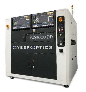
CyberOptics Corporation will unveil the new SQ3000-DD 3D AOI system with two Multi-Reflection Suppression (MRS) sensors at NEPCON South China, scheduled to take place August 29-31, 2017 at the Shenzhen Convention & Exhibition Center. CyberOptics will be at Booth 1J45.
The dual lane, dual sensor system is an extension of the award-winning SQ3000 3D AOI platform, deemed best in class. The new SQ3000-DD 3D AOI maximizes flexibility catering to varying PCB widths. This unique design provides the ability to inspect high volume assemblies, the convenience of inspecting different assemblies and board sizes simultaneously on different lanes, or even switching from dual lane to single lane mode to inspect very large boards.
Not only does the SQ3000-DD provide the PCB inspection flexibility, it also provides the flexibility to choose two of the same or two different proprietary MRS sensors, both of which meticulously identify and reject multiple reflections caused by shiny components and reflective solder joints. The new Ultra-High Resolution MRS sensor option provides an even finer resolution than the standard, delivering superior inspection performance ideally suited for 0201 metric and microelectronics applications where an even greater degree of accuracy and inspection reliability is critical. The unique architecture of both MRS sensor options simultaneously captures and transmits multiple images in parallel, while highly sophisticated 3D fusing algorithms merge the images together, delivering microscopic image quality at production speed.
"We have extended the MRS-enabled SQ3000 3D AOI platform to offer a dual lane, dual sensor solution," said Dr. Subodh Kulkarni, President and CEO, CyberOptics. "This flexibility will allow our customers to further increase their productivity with high volume throughput, while relying on the unprecedented combination of speed, accuracy and ease-of-use."
Also on display, the QX250i simultaneous double-sided AOI system offers fast, flexible and high performance inspection for all applications, and is ideally suited for pre-reflow and selective solder inspection. The top and bottom high-resolution Strobed Inspection Modules (SIMs) with enhanced illumination provide a single platform for the inspection and defect review process that shortens the production line and drives approximately 50 percent productivity improvement.
The SE600 3D SPI system delivers 'true' volume measurement and world-class usability. Designed with a state-of-the-art dual illumination sensor, it offers the best repeatability and reproducibility – even on the smallest paste deposits. The award-winning software offers full touch screen capability and world-class user experience for easy, flawless inspection.
About CyberOptics
CyberOptics Corporation is a leading global developer and manufacturer of high precision sensing technology solutions. CyberOptics sensors are being used in general purpose metrology and 3D scanning, surface mount technology (SMT) and semiconductor markets to significantly improve yields and productivity. By leveraging its leading edge technologies, the company has strategically established itself as a global leader in high precision 3D sensors, allowing CyberOptics to further increase its penetration of its key vertical markets. Headquartered in Minneapolis, Minnesota, CyberOptics conducts worldwide operations through its facilities in North America, Asia and Europe. For more information, click here.


