Laser Patterning & Metallization to Reduce Process Steps for PCB Manufacturing
August 29, 2017 | Joel Schrauben, Cameron Tribe, Christopher Ryder and Jan Kleinert, ELECTRO SCIENTIFIC INDUSTRIESEstimated reading time: 1 minute

Abstract
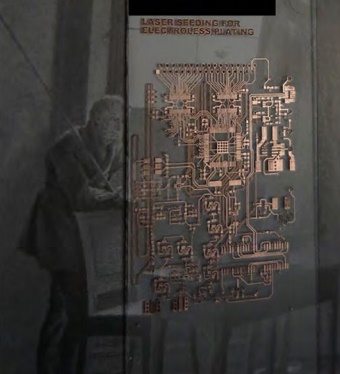
Glass offers a number of advantages as a dielectric material, such as a low coefficient of thermal expansion (CTE), high dimensional stability, high thermal conductivity and suitable dielectric constant. These properties make glass an ideal candidate for, among other things, package substrate and high-frequency PCB applications. We report here a novel process for the production of printed circuit boards and integrated circuit packaging using glass as both a dielectric medium and a platform for wiring simultaneously.
An ultrafast laser is used to etch away the desired pattern (pads, wires and vias) in the glass, and copper plating is “seeded” through the laser-based deposition of copper droplets. The seeded area is then plated using electroless plating followed by electroplating. Demonstrations of fine pitch wires, variable diameter through holes and blind vias, and a multilayer stack are shown. The deposits have a resistivity less than a factor of 1.5x that of bulk copper for 5-10 mm wires. Plated lines in borosilicate glass of 7-10 μm width and 5-20 μm depth and line spacing down to ~10 μm are demonstrated, as well as vias with a top diameter approaching 100 μm for 150 μm glass and 40 μm for 50 μm glass.
The process presents the potential for significant material savings in terms of base materials, process chemicals, and waste disposal/recycling costs (glass is on the order of 100-fold less expensive than some current high-frequency dielectrics, and wet processes account for a large part of standard PCB/substrate manufacturing). Additionally, the processes are amenable toward other dielectric materials such as FR-4, polyimide and PTFE-based materials.
Introduction
Increased demand for high data transmission rates is driving the development of smaller PCB features. Electrical circuits are reaching the physical limitations of traditional PCB dielectric materials under which electromagnetic compatibility can be controlled.
To read the full version of this article which appeared in the August 2017 issue of The PCB Magazine, click here.
Testimonial
"We’re proud to call I-Connect007 a trusted partner. Their innovative approach and industry insight made our podcast collaboration a success by connecting us with the right audience and delivering real results."
Julia McCaffrey - NCAB GroupSuggested Items
How Good Design Enables Sustainable PCBs
08/21/2025 | Gerry Partida, Summit InterconnectSustainability has become a key focus for PCB companies seeking to reduce waste, conserve energy, and optimize resources. While many discussions on sustainability center around materials or energy-efficient processes, PCB design is an often overlooked factor that lies at the heart of manufacturing. Good design practices, especially those based on established IPC standards, play a central role in enabling sustainable PCB production. By ensuring designs are manufacturable and reliable, engineers can significantly reduce the environmental impact of their products.
50% Copper Tariffs, 100% Chip Uncertainty, and a Truce
08/19/2025 | Andy Shaughnessy, I-Connect007If you’re like me, tariffs were not on your radar screen until a few months ago, but now political rhetoric has turned to presidential action. Tariffs are front-page news with major developments coming directly from the Oval Office. These are not typical times. President Donald Trump campaigned on tariff reform, and he’s now busy revamping America’s tariff policy.
Global PCB Connections: Understanding the General Fabrication Process—A Designer’s Hidden Advantage
08/14/2025 | Markus Voeltz -- Column: Global PCB ConnectionsDesigners don’t need to become fabricators, but understanding the basics of PCB fabrication can save you time, money, and frustration. The more you understand what’s happening on the shop floor, the better you’ll be able to prevent downstream issues. As you move into more advanced designs like HDI, flex circuits, stacked vias, and embedded components, this foundational knowledge becomes even more critical. Remember: the fabricator is your partner.
MKS’ Atotech to Participate in IPCA Electronics Expo 2025
08/11/2025 | AtotechMKS Inc., a global provider of enabling technologies that transform our world, announced that its strategic brands ESI® (laser systems) and Atotech® (process chemicals, equipment, software, and services) will showcase their latest range of leading manufacturing solutions for printed circuit board (PCB) and package substrate manufacturing at the upcoming 17th IPCA Show to be held at Pragati Maidan, New Delhi from August 21-23, 2025.
MKS Showcases Next-generation PCB Manufacturing Solutions at the Thailand Electronics Circuit Asia 2025
08/06/2025 | MKS Instruments, Inc.MKS Inc, a global provider of enabling technologies that transform our world, today announced its participation in Thailand Electronics Circuit Asia 2025 (THECA 2025), taking place August 20–22 at BITEC in Bangkok.