Gardien Services USA Announces Tiger AVI Machine for Demonstration
September 15, 2017 | Gardien Services USAEstimated reading time: 1 minute

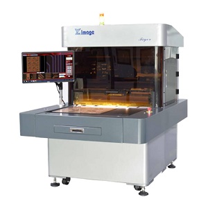
Gardien Services USA announces the placement of a Tiger AVI inspection machine to their Anaheim California Test Center.
The new system is available for demonstration and evaluation using your own product. Our Tiger system is able to scan your final product with two RGB CCD cameras utilizing pixel resolution down to 25 micron. With Tigers 6.3”/second single side scan rate your product is processed expediently and efficiently.
Tiger is able to scan for defects such as Foreign Material Inclusion, Legend defects, Dishdowns, Exposed Copper, Soldermask defects, Mouse Bites and many others. Tiger inspects many surface finishes including HASL, Immersion Silver and Gold, Bare Copper, OSP and others.
The Tiger processes your Gerber Data in order to provide Image Contrast Comparison with logic analysis. The Tiger system can also provide AOI services by a simple software switch.
The Tiger’s high speed, AVI/AOI combination, CCD cameras, and large table size are but a few items that make Tiger stand out as your “Go-To” solution for final board inspection and alternative AOI.
About Gardien
The Gardien Group is the world’s largest provider of independent quality assurance services to the PCB board shops and large international fabricators. Gardien’s specialized quality assurance and quality control services help clients free up their resources to focus on what they do best, “the production of class leading printed circuit boards.” Gardien’s 25 facilities located throughout Asia, North America and Europe, to fully integrated inspection within a PCB production environment, Gardien’s 500 employees serve customers supplying the automotive, defense, telecommunications, aerospace, medical, computer, and industrial markets worldwide.
For more information, click here.
Testimonial
"We’re proud to call I-Connect007 a trusted partner. Their innovative approach and industry insight made our podcast collaboration a success by connecting us with the right audience and delivering real results."
Julia McCaffrey - NCAB GroupSuggested Items
Trouble in Your Tank: Implementing Direct Metallization in Advanced Substrate Packaging
09/15/2025 | Michael Carano -- Column: Trouble in Your TankDirect metallization systems based on conductive graphite are gaining popularity throughout the world. The environmental and productivity gains achievable with this process are outstanding. Direct metallization reduces the costs of compliance, waste treatment, and legal issues related to chemical exposure. A graphite-based direct plate system has been devised to address these needs.
Closing the Loop on PCB Etching Waste
09/09/2025 | Shawn Stone, IECAs the PCB industry continues its push toward greener, more cost-efficient operations, Sigma Engineering’s Mecer System offers a comprehensive solution to two of the industry’s most persistent pain points: etchant consumption and rinse water waste. Designed as a modular, fully automated platform, the Mecer System regenerates spent copper etchants—both alkaline and acidic—and simultaneously recycles rinse water, transforming a traditionally linear chemical process into a closed-loop system.
Driving Innovation: Depth Routing Processes—Achieving Unparalleled Precision in Complex PCBs
09/08/2025 | Kurt Palmer -- Column: Driving InnovationIn PCB manufacturing, the demand for increasingly complex and miniaturized designs continually pushes the boundaries of traditional fabrication methods, including depth routing. Success in these applications demands not only on robust machinery but also sophisticated control functions. PCB manufacturers rely on advanced machine features and process methodologies to meet their precise depth routing goals. Here, I’ll explore some crucial functions that empower manufacturers to master complex depth routing challenges.
Trouble in Your Tank: Minimizing Small-via Defects for High-reliability PCBs
08/27/2025 | Michael Carano -- Column: Trouble in Your TankTo quote the comedian Stephen Wright, “If at first you don’t succeed, then skydiving is not for you.” That can be the battle cry when you find that only small-diameter vias are exhibiting voids. Why are small holes more prone to voids than larger vias when processed through electroless copper? There are several reasons.
The Government Circuit: Navigating New Trade Headwinds and New Partnerships
08/25/2025 | Chris Mitchell -- Column: The Government CircuitAs global trade winds continue to howl, the electronics manufacturing industry finds itself at a critical juncture. After months of warnings, the U.S. Government has implemented a broad array of tariff increases, with fresh duties hitting copper-based products, semiconductors, and imports from many nations. On the positive side, tentative trade agreements with Europe, China, Japan, and other nations are providing at least some clarity and counterbalance.