


 Trouble in Your Tank: Implementing Direct Metallization in Advanced Substrate Packaging
 It’s Only Common Sense: Storytelling That Sells—Stop Pitching, Start Painting Pictures
 The Right Approach: Get Ready for ISO 9001 Version 6


Semiconductor Patterning of Seven Nanometers Technology Using a Camera Flash
September 20, 2017 | KAISTEstimated reading time: 2 minutes
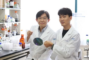
A research team led by Professor Sang Ouk Kim in the Department of Materials Science and Engineering at KAIST has developed semiconductor manufacturing technology using a camera flash.
This technology can manufacture ultra-fine patterns over a large area by irradiating a single flash with a seven-nanometer patterning technique for semiconductors. It can facilitate the manufacturing of highly efficient, integrated semiconductor devices in the future.
Technology for the Artificial Intelligence (AI), the Internet of Things (IoTs), and big data, which are the major keys for the fourth Industrial Revolution, require high-capacity, high-performance semiconductor devices. It is necessary to develop lithography technology to produce such next-generation, highly integrated semiconductor devices.
20170918143400_25291_1504586573.jpg
Although related industries have been using conventional photolithography for small patterns, this technique has limitations for forming a pattern of sub-10 nm patterns.
Molecular assembly patterning technology using polymers has been in the spotlight as the next generation technology to replace photolithography because it is inexpensive to produce and can easily form sub-10 nm patterns. However, since it generally takes a long time for heat treatment at high-temperature or toxic solvent vapor treatment, mass production is difficult and thus its commercialization has been limited.
The research team introduced a camera flash that instantly emits strong light to solve the issues of polymer molecular assembly patterning. Using a flash can possibly achieve a semiconductor patterning of seven nanometers within 15 milliseconds (1 millisecond = 1/1,000 second), which can generate a temperature of several hundred degrees Celsius in several tens of milliseconds.
The team has demonstrated that applying this technology to polymer molecular assembly allows a single flash of light to form molecular assembly patterns.
Formation of semiconductor patterns using a camera flash)
The team also identified its compatibility with polymer flexible substrates, which are impossible to process at high temperatures. Through these findings, the technology can be applied to the fabrication of next-generation, flexible semiconductors.
The researchers said the camera flash photo-thermal process will be introduced into molecular assembly technology and this highly-efficiency technology can accelerate the realization of molecular assembly semiconductor technology.
Schematic diagram of molecular assembly pattern using a camera flash
Professor Kim, who led the research, said, “Despite its potential, molecular assembly semiconductor technology has remained a big challenge in improving process efficiency.” “This technology will be a breakthrough for the practical use of molecular assembly-based semiconductors.”
The paper was published in the international journal, Advanced Materials on August 21 with first authors, researcher Hyeong Min Jin and PhD candidate Dae Yong Park.
The research, sponsored by the Ministry of Science and ICT, was co-led Professor by Keon Jae Lee in the Department of Materials Science and Engineering at KAIST, and Professor Kwang Ho Kim in the School of Materials Science and Engineering at Pusan National University.
Share on:


Testimonial
"The I-Connect007 team is outstanding—kind, responsive, and a true marketing partner. Their design team created fresh, eye-catching ads, and their editorial support polished our content to let our brand shine. Thank you all! "
Sweeney Ng - CEE PCBSuggested Items
Altair, Wichita State University’s NIAR Sign MoU to Accelerate Aerospace Innovation
09/16/2025 | AltairAltair, a global leader in computational intelligence, and Wichita State University’s (WSU) National Institute for Aviation Research (NIAR), one of the world’s leading aerospace research institutions, have signed a memorandum of understanding (MoU) to advance innovation across the aerospace and defense industries.
AI-Powered Wearables Transform How Consumers Interact with Everyday Technology
09/15/2025 | PR NewswireThe global demand for AI-driven, touchless wearable technologies is accelerating as consumers seek more natural, seamless and intuitive ways to interact with their devices. Traditional touch screens and voice assistants, while effective, are increasingly viewed as limiting in a world where multitasking, mobility and efficiency are key. As industries from consumer electronics to augmented reality and enterprise computing embrace the possibilities of gesture-based control, the market for neural interfaces is rapidly expanding
Hanwha Aerospace to Collaborate with BAE Systems on Advanced Anti-jamming GPS for Guided Missiles
09/15/2025 | HanwhaHanwha Aerospace has signed a contract with BAE Systems to integrate next-generation, anti-jamming Global Positioning System (GPS) technology into Hanwha Aerospace’s Deep Strike Capability precision-guided weapon system.
United Electronics Corporation Unveils Revolutionary CIMS Galaxy 30 Automated Optical Inspection System
09/11/2025 | United Electronics CorporationUnited Electronics Corporation (UEC) today announced the launch of its new groundbreaking CIMS Galaxy 30 Automated Optical Inspection (AOI) machine, setting a new industry standard for precision electronics manufacturing quality control. The Galaxy 30, developed and manufactured by CIMS, represents a significant leap forward in inspection technology, delivering exceptional speed improvements and introducing cutting-edge artificial intelligence capabilities.
Intel Announces Key Leadership Appointments to Accelerate Innovation and Strengthen Execution
09/09/2025 | Intel CorporationIntel Corporation today announced a series of senior leadership appointments that support the company’s strategy to strengthen its core product business, build a trusted foundry, and foster a culture of engineering across the business.