


 Dan’s Biz Bookshelf: ‘Abundance: How We Build a Better Future’
 Trouble in Your Tank: In Complex Systems, Design Rules Aren’t Optional
 It’s Only Common Sense: The Phone Is Still Your Competitive Advantage


Deca Announces Agreement with IBM to Bring High-Density Fan-Out Interposer Production to North America
May 20, 2025 | Deca TechnologiesEstimated reading time: 2 minutes
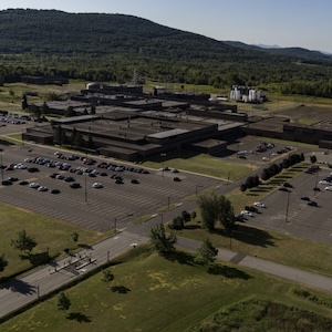
Deca Technologies announced the signing of an agreement with IBM to implement Deca’s M-Series™ and Adaptive Patterning® technologies in IBM’s advanced packaging facility in Bromont, Quebec. Through the agreement, IBM will implement a high-volume manufacturing line with a focus on Deca’s M-Series Fan-out Interposer Technology (MFIT™).
This collaboration builds on IBM’s strategy to develop its advanced packaging capabilities. IBM Canada's plant in Bromont is one of North America’s largest semiconductor assembly and test sites and has been at the forefront of packaging innovation for over five decades. Recent investments to expand the site’s capabilities have positioned it as a critical hub for high-performance packaging and chiplet integration, supporting technologies like MFIT that are essential for AI, HPC, and data center applications.
Deca’s M-Series platform is the highest-volume fan-out packaging technology in the world, with over seven billion M-Series units shipped. MFIT builds on this proven foundation by integrating embedded bridge die for chips’ last processor and memory integration delivering high-density, low-latency connections between chiplets. MFIT provides a cost-effective alternative to full silicon interposers, offering improved signal integrity, greater design flexibility, and the scalable format needed for ever-larger AI, HPC, and data center devices.
This cooperation reflects the shared commitment of IBM and Deca to advance the next generation of semiconductor packaging. By combining IBM’s advanced packaging capabilities with Deca’s proven technology, the two companies are expanding the global supply chain for the future of high-performance chiplet integration and advanced computing systems.
“Advanced packaging and chiplet technology are critical for faster, more efficient computing solutions in the age of AI. Deca will help ensure IBM’s Bromont facility remains at the forefront of these innovations, strengthening our commitment to helping our clients bring products to market faster and deliver better performance for AI and data-heavy applications,” said Scott Sikorski, Head of Business Development for Chiplets & Advanced Packaging at IBM.
“IBM’s rich history in semiconductor innovation and advanced packaging makes them an ideal partner to bring MFIT to high-volume production,” said Tim Olson, Founder and CEO of Deca. “We are thrilled to be working together to bring this advanced interposer technology to the North American ecosystem.”
Share on:


Subscribe
Stay ahead of the technologies shaping the future of electronics with our latest newsletter, Advanced Electronics Packaging Digest. Get expert insights on advanced packaging, materials, and system-level innovation, delivered straight to your inbox.
Subscribe now to stay informed, competitive, and connected.
Suggested Items
SEMI 3D & Systems Summit to Advance AI, Hybrid Bonding, and Chiplet Ecosystem
05/06/2026 | SEMIGlobal experts in advanced semiconductor packaging and 3D integration will convene at the annual SEMI 3D & Systems Summit, June 17–19, 2026, in Dresden, Germany.
AI Interconnect Boom Drives Southeast Asia Outsourcing Expansion
05/05/2026 | TrendForceGlobal shipment volume of optical transceivers is projected to more than triple from 26.5 million units in 2023 to over 92 million units by 2026, according to TrendForce’s latest AI infrastructure research.
U.S. Semiconductor Industry Convenes at Glass4Chips Summit
05/04/2026 | NY CREATESThe 2026 Glass4Chips Summit will bring together leaders and innovators across industry, academia, and government to address a framework for accelerating the adoption of glass substrates in next-generation semiconductor manufacturing and packaging.
SCHMID Launches 'Any Layer ET' for Panel-Level Advances Packaging, to Present at ECTC 2026
04/30/2026 | SCHMID GroupSCHMID Group, a global leader in advanced manufacturing solutions for the electronics and semiconductor industries, is advancing next-generation substrate manufacturing with its proprietary Any Layer ET (Embedded Trace) Process for full panel-level Advanced Packaging.
AI Competition Turns into a Supply Chain Arms Race, Tightening Advanced Packaging and 3nm Capacity
04/30/2026 | TrendForceTrendForce’s latest foundry industry findings point out that AI demand has surged rapidly since 2023, leading to capacity bottlenecks in 3 nm–2 nm wafers and 2.5D/3D advanced packaging.