-
- News
- Books
Featured Books
- smt007 Magazine
Latest Issues
Current IssueWhat's Your Sweet Spot?
Are you in a niche that’s growing or shrinking? Is it time to reassess and refocus? We spotlight companies thriving by redefining or reinforcing their niche. What are their insights?
Moving Forward With Confidence
In this issue, we focus on sales and quoting, workforce training, new IPC leadership in the U.S. and Canada, the effects of tariffs, CFX standards, and much more—all designed to provide perspective as you move through the cloud bank of today's shifting economic market.
Intelligent Test and Inspection
Are you ready to explore the cutting-edge advancements shaping the electronics manufacturing industry? The May 2025 issue of SMT007 Magazine is packed with insights, innovations, and expert perspectives that you won’t want to miss.
- Articles
- Columns
- Links
- Media kit
||| MENU - smt007 Magazine
Goepel electronic's New Detector for Flexible Automated X-ray Inspection
November 6, 2017 | GOEPEL ElectronicEstimated reading time: 1 minute

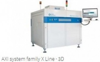
Goepel electronic's StingRay Detector is the name of the new image acquisition concept for fully automatic X-ray inspection of single-sided and double-sided PCBs. It enables selective 2D, 2.5D and 3D X-ray inspection with high image quality at highest speed. The StingRay Detector is another option for the inline AXI systems of the X Line · 3D family.
The new technology ensures even better layer separation and brilliant, high-resolution images, especially on 3D images of selected areas. The detector concept consisting of a high-speed X/Y axis and a flat-panel detector keeps the balance between image quality and cycle time. The focus is on the reliable inspection of challenging solder joints such as BGAs, QFNs and LGAs. By a scalable number of acquired projections, a high quality of the layer separation is achieved. The 3D reconstruction of the images is done by the planar CT.
The StingRay Detector can be configured according to the inspection task. For example, a total of three detector sizes with a resolution of 1.3 to 6 megapixels are available. In addition to the stepless height adjustment of the X-ray source, the detector distance to the module can also be varied in three steps. This results in different image field sizes and resolutions depending on the specific requirements.
The StingRay Detector addresses users with a test strategy that requires reliable inspection of individual assembly areas at top speed. In contrast to this, the MultiAngle Detector for the X Line · 3D family realizes a full-surface X-ray inspection of all solder joints on the entire board with a scanning image acquisition.
Suggested Items
Driving Innovation: Direct Imaging vs. Conventional Exposure
07/01/2025 | Simon Khesin -- Column: Driving InnovationMy first camera used Kodak film. I even experimented with developing photos in the bathroom, though I usually dropped the film off at a Kodak center and received the prints two weeks later, only to discover that some images were out of focus or poorly framed. Today, every smartphone contains a high-quality camera capable of producing stunning images instantly.
Hands-On Demos Now Available for Apollo Seiko’s EF and AF Selective Soldering Lines
06/30/2025 | Apollo SeikoApollo Seiko, a leading innovator in soldering technology, is excited to spotlight its expanded lineup of EF and AF Series Selective Soldering Systems, now available for live demonstrations in its newly dedicated demo room.
Indium Corporation Expert to Present on Automotive and Industrial Solder Bonding Solutions at Global Electronics Association Workshop
06/26/2025 | IndiumIndium Corporation Principal Engineer, Advanced Materials, Andy Mackie, Ph.D., MSc, will deliver a technical presentation on innovative solder bonding solutions for automotive and industrial applications at the Global Electronics A
Fresh PCB Concepts: Assembly Challenges with Micro Components and Standard Solder Mask Practices
06/26/2025 | Team NCAB -- Column: Fresh PCB ConceptsMicro components have redefined what is possible in PCB design. With package sizes like 01005 and 0201 becoming more common in high-density layouts, designers are now expected to pack more performance into smaller spaces than ever before. While these advancements support miniaturization and functionality, they introduce new assembly challenges, particularly with traditional solder mask and legend application processes.
Knocking Down the Bone Pile: Tin Whisker Mitigation in Aerospace Applications, Part 3
06/25/2025 | Nash Bell -- Column: Knocking Down the Bone PileTin whiskers are slender, hair-like metallic growths that can develop on the surface of tin-plated electronic components. Typically measuring a few micrometers in diameter and growing several millimeters in length, they form through an electrochemical process influenced by environmental factors such as temperature variations, mechanical or compressive stress, and the aging of solder alloys.