


 Fresh PCB Concepts: Key Considerations for Reliability, Performance, and Compliance in PCBs
 Elementary Mr. Watson: Navigating RF—A Glide Path Approach to Design Success
 Designers Notebook: Layer Stackup Planning for RF Circuit Boards


Happy Holden and Charles Pfeil Discuss the Past and Future of PCB Design, Part 1
November 7, 2017 | Barry Matties, I-Connect007Estimated reading time: 10 minutes
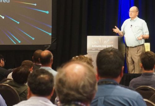
When it comes to the PCB design community and the challenges facing it, as well as where design has been and where it’s heading, there aren’t many people as qualified to speak on the topic as long-time industry veterans Happy Holden and Charles Pfeil. I joined Happy and Charles at the recent AltiumLive 2017 event in San Diego for a discussion about the current state of PCB design, what the future holds, and what it means to be a designer.
BARRY MATTIES: You both have been in the industry for a number of years. Tell me about how you got your start. Charles, let’s begin with you.
CHARLES PFEIL: I started working summers when I was in high school, so 1966. My first job was doing QA on Rubylith designs for Northrop. Then I eventually became a designer and I job-shopped for probably about 14 years before I started my own service firm.
MATTIES: So it was always design then?
PFEIL: Always design, yeah.
MATTIES: When did you two meet?
HAPPY HOLDEN: Mentor?
PFEIL: No, before Mentor. We probably met at trade shows prior to Mentor. I'm sure of that.
MATTIES: There's a lot of history between the two of you.
HOLDEN: Lost in antiquity. You should've asked us 10 years ago. We would've remembered (laughs).
PFEIL: I was writing my book around 2005, so I know we met before that.
MATTIES: In any case, you started out with circuit design. That was how many years ago?
PFEIL: It was 51 years ago.
MATTIES: What's the most dramatic change that you've seen in circuit board design?
PFEIL: I think it's the impact of miniaturization, the impact of high-speed circuits, and the impact of new fabrication technologies. One of the difficulties has always been keeping up with that, especially with software design. When developing software, we'll start working on something to support a new technology and then, before you know it, it's moved on to some other technology before that method has matured. That's why so often the software companies are behind the curve when it comes to keeping up with technology and fabrication changes.
MATTIES: When you say the impact of miniaturization, what sort of impact do you mean?
PFEIL: The type of design solutions that used to be valid became invalid. A great example was when grids were no longer a valid method for primary routing. When they switched over to surface mount and you had to go between the pins and you're not on a grid, I was working at ASI at that time. We had to make significant enhancements to support that technology. All the algorithms were based on a grid, so you could have a rather rough minimum resolution. But as soon as you go gridless, you've got to have a very fine resolution, which means all the algorithms would no longer work effectively. So that was a big change.
MATTIES: What do you think the greatest challenge is today in PCB design?
PFEIL: I think understanding high-speed circuits and designing them in a way that they'll behave as desired.
MATTIES: I was just listening to Max Seeley, the gentleman from 3M. He's one of the keynotes here. He said it's really the EEs that are going to become circuit designers.
PFEIL: I think Happy would agree with me that the designers who have experience with manual design are retiring or passing away. The good news is that most of the ones coming up behind them have electronics education. They know circuit design. They choose to do PCB design, like Rick Hartley, a great example. For them, the design is really a big challenge, but because they understand the circuit side better, I think it's easier for them.
MATTIES: The tool certainly makes it easier.
PFEIL: But for a circuit engineer to go into design and not understand the fabrication process and or how to constrain it properly and not over-constrain it, that's a challenge.
MATTIES: One of the things that we often hear, and you just mentioned it, is designers not understanding the manufacturing process. I hear that frequently. Is it really their job to understand the manufacturing process, or is their job to get feedback from the manufacturing process?
HOLDEN: I for a long time have advocated that it's useful for designer to get a tour of a PC board shop and sit down with the fabricators. But for a designer magically to understand the nuances of what takes a process engineer an entire career to learn, they're not going to learn in one hour. You're deluding yourself if you think you're going to give these designers this two-hour tour of how PC boards are made and they're never going to make a mistake again.
Page 1 of 2
Share on:


Suggested Items
Murata Manufacturing Vietnam Expands Ho Chi Minh Plant with New Production Building
05/08/2025 | MurataMurata Manufacturing Vietnam Co., Ltd. (Ho Chi Minh, Vietnam), a manufacturing subsidiary of Murata Manufacturing Co., Ltd., will begin construction on a new production building at its Ho Chi Minh plant in May 2025.
LG Electronics India Limited Begins Construction of Its Third Manufacturing Plant in India
05/08/2025 | BUSINESS WIRELG Electronics India Ltd. (LGEIL) announced the commencement of construction of its new manufacturing facility in Sri City, Andhra Pradesh today at a ceremony graced by the presence of Shri Nara Lokesh, Hon'ble Minister for Information Technology, Electronics and Communications.
Scanfil Boosts Investment in Electronics Manufacturing in the US
05/08/2025 | BUSINESS WIREScanfil is investing in a second electronics manufacturing line in Atlanta, Georgia, USA. The demand for manufacturing electronics in the USA has increased over the past two years and is expected to continue growing.
Nortech Systems Unveils Reimagined Brand Identity
05/08/2025 | Nortech SystemsNortech Systems Incorporated, a leading provider of engineering and manufacturing solutions for complex electromedical and electromechanical products serving the medical, industrial and defense markets, is proud to unveil its newly refreshed brand, "Connections Reimagined."
MKS Breaks Ground on New Chemical Manufacturing and TechCenter Facility in Thailand
05/07/2025 | MKS Instruments, Inc.MKS Instruments. Inc., a global provider of enabling technologies that transform our world, announced today the groundbreaking of its cutting-edge Atotech chemical manufacturing and TechCenter facility at the Asia Industrial Estate Suvarnabhumi, located east of Bangkok, Thailand.