


 Standard of Excellence: The Future of Fabrication—From Art to Automation
 Knocking Down the Bone Pile: The Business Case for Component Reclamation
 Global Sourcing Spotlight: The Hidden Power of the Rep Network


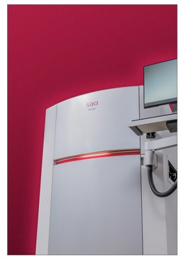
Saki Corporation, an innovator in the field of automated optical and x-ray inspection systems, will introduce its new 3Di AOI systems at productronica 2017, which will be held from November 14-17 in Munich, Germany. Saki will be in Stand A2.259.
The new system delivers high-speed (5,700mm2/sec), high-accuracy (XY positioning of 3µm at 3Ơ), height repeatability (below 2µm at 3Ơ), and scalable resolutions of 7, 12 and 18µm for boards weighing 12kg.
Saki's rigid gantry structure is a key component of the 3Di-LS2, 3Di-LD2, and 3Di-ZS2 hardware platforms. A dual-motor drive system, linear scale, and full closed-loop functionality provide machine accuracy and repeatability to generate absolute measurement data, which is essential for accurate machine-2-machine (M2M) communication. Saki's CoaXPress interface in the overhead camera captures images 1.7 times faster than previous models.
On display will also be Saki's new 3D solder paste inspection (SPI) systems, the 3Si-LS2, 3Si-LD2, and 3Si-7µm. One common software platform supports all Saki 3D inspection systems - solder paste, optical, and x-ray--with an easy-to-program, intuitive software wizard. Auto-programming software significantly reduces library creation time, as libraries are automatically created using Gerber and CAD data. Algorithm-based software provides extensive programming capabilities, even for non-programmers. Saki's inspection data and default thresholds adhere to IPC standards.
Saki is also introducing its new concept, Quality Driven Production, or QDP. QDP is a set of tools that ensures that the data and information that is communicated to third party systems is valid and accurate. It improves the stability of the process, while at the same time it increases productivity and minimizes the operating cost of the equipment. A self-diagnostic system with predictive and preventive maintenance management assures stable machine conditions and repeatable, consistent performance. Every key component is monitored along with system conditions, and a detailed diagnostic log is recorded. An optimized preventive maintenance plan reduces maintenance time, machine down-time, manpower, and costs.
The Multi Process View (MPV) on the BF2-Monitor shows the results of all inspection processes (SPI, pre-reflow, and post reflow) on one screen in real time for operator review, simplifying the verification process and making it less subject to error. It is also useful for analyzing the cause of a defective board.
"We are excited to introduce our new 3D AOI and 3D SPI systems to the industry at Productronica and to discuss our Smart Factory/Industry 4.0 initiatives and partnerships," said Katsuhiro Eddie Ichiyama, General Manager of SAKI Europe. "In addition to these systems, we will also be displaying Saki's 3D automated x-ray inspection (3D AXI) for circuit boards in applications that are too critical to fail."
About Saki
Since its inception in 1994, Saki has led the way in the development of automated recognition through robotic vision technology. Saki's 3D automated solder paste, optical, and x-ray inspection systems (SPI, AOI, AXI) have been recognized to provide the stable platform and advanced data capture mechanisms necessary for true M2M communication, improving production, process efficiency, and product quality. Saki Corporation has headquarters in Tokyo, Japan with offices, sales, and support centers around the world.


