


 Trouble in Your Tank: Implementing Direct Metallization in Advanced Substrate Packaging
 It’s Only Common Sense: Storytelling That Sells—Stop Pitching, Start Painting Pictures
 The Right Approach: Get Ready for ISO 9001 Version 6


Watching Atoms Move in Hybrid Perovskite Crystals Reveals Clues to Improving Solar Cells
November 27, 2017 | UC San DiegoEstimated reading time: 2 minutes
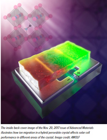
A team of researchers led by the University of California San Diego has for the first time observed nanoscale changes deep inside hybrid perovskite crystals that could offer new insights into developing low-cost, high-efficiency solar cells.
Using X-ray beams and lasers, researchers studied how a new promising class of solar cell materials, called hybrid perovskites, behaves at the nanoscale level during operation. Their experiments revealed that when voltage is applied, ions migrate within the material, creating regions that are no longer as efficient at converting light to electricity.
“Ion migration hurts the performance of the light absorbing material. Limiting it could be a key to improving the quality of these solar cells,” said David Fenning, a professor of nanoengineering and member of the Sustainable Power and Energy Center at UC San Diego.
The team, led by Fenning, includes researchers from the AMOLF Institute in the Netherlands and Argonne National Laboratory. Researchers published their findings in Advanced Materials.
Hybrid perovskites are crystalline materials made of a mixture of both inorganic and organic ions. They are promising materials for making next-generation solar cells because they are inexpensive to manufacture and are considerably efficient at converting light to electricity.
However, hybrid perovskites are not very stable, which can make them difficult to study. Microscopic techniques typically used to study solar cells often end up damaging the hybrid perovskites or can’t image beyond their surfaces.
Now, a UC San Diego-led team has shown that by using a technique called nanoprobe X-ray fluorescence, they can probe deep into hybrid perovskite materials without destroying them. “This is a new window to peer inside these materials and see precisely what’s going wrong,” Fenning said.
The researchers studied a type of hybrid perovskite called methylammonium lead bromide, which contains negatively charged bromine ions. Like other hybrid perovskites, its crystalline structure contains many vacancies, or missing atoms, which have been suspected to allow ions to move readily within the material when a voltage is applied.
The researchers first performed nanoprobe X-ray fluorescence measurements on the crystals to create high-resolution maps of the atoms inside the material. The maps revealed that when voltage is applied, the bromine ions migrate from negatively charged areas to positively charged areas.
Next, the researchers shined a laser on the crystals to measure a property called photoluminescence—the material’s ability to emit light when excited by a laser—in different areas of the crystals. A good solar cell material emits light very well, so the higher the photoluminescence, the more efficient the solar cell should be. The areas with higher bromine concentrations had up to 180 percent higher photoluminescence than areas depleted of bromine ions.
“We watch the bromine ions migrate within minutes and see that the resulting bromine-rich areas have the potential to become better solar cells while the performance is degraded in bromine-poor areas,” Fenning said.
Fenning and his team are now exploring ways to limit bromine migration in methylammonium lead bromide and other hybrid perovskites. Researchers say that one potential option would be growing hybrid perovskite crystals in different conditions to minimize the number of vacancies and limit ion migration in the crystalline structure.
Share on:


Testimonial
"In a year when every marketing dollar mattered, I chose to keep I-Connect007 in our 2025 plan. Their commitment to high-quality, insightful content aligns with Koh Young’s values and helps readers navigate a changing industry. "
Brent Fischthal - Koh YoungSuggested Items
September 2025 PCB007 Magazine: The Future of Advanced Materials
09/16/2025 | I-Connect007 Editorial TeamMoore’s Law is no more, and the advanced material solutions being developed to grapple with this reality are surprising, stunning, and perhaps a bit daunting. Buckle up for a dive into advanced materials and a glimpse into the next chapters of electronics manufacturing.
I-Connect007 Launches Advanced Electronics Packaging Digest
09/15/2025 | I-Connect007I-Connect007 is pleased to announce the launch of Advanced Electronics Packaging Digest (AEPD), a new monthly digital newsletter dedicated to one of the most critical and rapidly evolving areas of electronics manufacturing: advanced packaging at the interconnect level.
Panasonic Industry will Double the Production Capacity of MEGTRON Multi-layer Circuit Board Materials Over the Next Five Years
09/15/2025 | Panasonic Industry Co., Ltd.Panasonic Industry Co., Ltd., a Panasonic Group company, announced plans for a major expansion of its global production capacity for MEGTRON multi-layer circuit board materials today. The company plans to double its production over the next five years to meet growing demand in the AI server and ICT infrastructure markets.
Trouble in Your Tank: Implementing Direct Metallization in Advanced Substrate Packaging
09/15/2025 | Michael Carano -- Column: Trouble in Your TankDirect metallization systems based on conductive graphite are gaining popularity throughout the world. The environmental and productivity gains achievable with this process are outstanding. Direct metallization reduces the costs of compliance, waste treatment, and legal issues related to chemical exposure. A graphite-based direct plate system has been devised to address these needs.
Fresh PCB Concepts: Designing for Success at the Rigid-flex Transition Area
08/28/2025 | Team NCAB -- Column: Fresh PCB ConceptsRigid-flex PCBs come in all shapes and sizes. Manufacturers typically use fire-retardant, grade 4 (FR-4) materials in the rigid section and flexible polyimide materials in the flex region. Because of the small size, some rigid-flex PCBs, like those for hearing aid devices, are among the most challenging to manufacture. However, regardless of its size, we should not neglect the transition area between the rigid and flexible material.