


 Knocking Down the Bone Pile: Revamp Your Components with BGA Reballing
 Global Sourcing Spotlight: Balancing Speed and Flexibility Without Sacrificing Control
 SMT Perspectives & Prospects: Artificial Intelligence Part 6: Data Module 1


DFx on High-Density Assemblies
December 1, 2017 | Jonas Sjoberg, Chris Nash, David Sbiroli, and Wisdom Qu, Indium CorporationEstimated reading time: 4 minutes
There are many ways to increase packaging density. Examples of technologies include fine-pitch connectors, package-on-package (PoP), fine pitch CSPs, 01005, 0201, and reduced component- to-component spacing.
Use of new technologies poses a number of challenges for solder paste selection, PCB design, assembly process, and reliability. The type of end product will have different challenges, concerns, and requirements in all aspects. The assembly line for many of these end products will look very similar, but specification limits would be different. Typical reliability tests are drop test, vibration, thermal cycling test (TCT), and SIR; even if the names of the tests are the same, the pass/fail criteria vary between different end products.
When it comes to material selection—and solder paste in particular—the type of end product plays a big role. An automotive, computing server, or router product would, in many cases, require an in-circuit test (ICT); thereby, the solder paste residues must be easy to penetrate with a test probe. A consumer product, on the other hand, typically doesn’t focus on ICT. The concern is more on throughput, thereby requiring a solder paste that is capable of fast screen printing.
There are many more examples, but with the increased need for high-density assembly, most, if not all, solder pastes must be able to print well on stencil apertures with area ratios (AR) way below the typical industry standard of 0.66. The AR for some products could be as low as 0.5-.55.
With the above challenges, finer solder powder is increasingly being used, and the type of solder powder is moving from type 3 towards type 4-4.5, and even type 5 for a number of applications. This poses some new challenges. In addition, low-silver and low-temperature alloys are gaining traction, making the selection of solder pastes and alloys more complex.
Once the correct solder paste material is selected, a feasible and robust assembly process must be developed and sustained. The assembly process ranges from screen-printing, placement, and reflow soldering in air or nitrogen to electrical and functional testing. Many factors influence the quality of the assembly process. With the reduced pitch and component spacing, the capabilities for solder paste, assembly, and PCB fabrication will be tested to its limits and beyond, with the need for using statistical tools is becoming a requirement to develop and maintain good yields.
Even with the right solder paste selection, good assembly process, and high-quality PCB and components, failures still will occur, leading to yield losses and extra cost. Once these failures occur, it is very easy to jump to conclusions and start making changes without knowing the root cause of the failure. As engineers, we quite often tend look for the most difficult solution, but in many cases, the simple solution is the right solution to solve the issue.
PCB and PCBA Design
When moving to high-density assembly, it is very important to understand PCB design and its limitations. With increasing density, the PCB fabrication becomes much more challenging. Some of the key PCB design requirements include:
• 50 μm copper/copper spacing (inner and outer layers)
• 50 μm solder mask slivers
• 25-40 μm solder mask registration tolerance
• 60 μm microvias
• 200 μm microvia capture pads in outer and inner layers
Understanding DFx and design is in many cases critical to be able to identify the root cause of the issues that occur on the production line. When it comes to PCB and PCBA design, there are many important aspects. In this paper, we have selected a few that have a critical impact on SPI and overall yields.
• PCB stretch and shrink
• Filled vs. unfilled microvias
• Silkscreen
PCB Stretch and Shrink
The maximum PCB stretch is 0.05 mm over the entire panel, and this must be clearly specified on the PCB fabrication drawing. This is very important for fine-pitch parts and high-density spacing products. The pads and apertures for 01005 passives and 0.3 mm pitch CSPs is 0.2 mm; a stretch or shrink of more than 0.05 mm leads to solder paste that will be 25% of the pad.
Microvia Issue
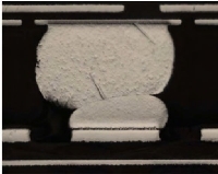
Excessive voids in some cases lead to solder bridging. This could be caused by oversized or "leaking" microvias in pad in combination with normal process variations. An issue on a smartphone can be seen below; failure rate for bridging was 6% in this case (Figure 2).
One primary issue today is that there are no clear specifications as to how big the microvias are allowed to be or where to measure the actual size of the microvia (Figure 4). Since there is no clear specification, the microvias can look different in size and shape between different suppliers and between batches of PCBs.
By filling the microvias with copper in the PCB fabrication process, the voids and bridging issues can be eliminated.
Silkscreen Issue
Depending on the quality of the silkscreen, the height on top of the solder mask could range from 15-40 μm. This can create a gap between the stencil and PCB of 15-40 μm, depending on the PCB design. The gap can create printing issues leading to both too little or too much solder paste height and volume. Depending on the design of a product, the solder mask can add 10-25 μm in addition to the silkscreen, creating a gap of 15-65 μm from the bottom of the stencil to the pad.
In this case, the top of the solder mask is 422 μm on top of the copper pad.
When the stencil is placed on top of the PCB, the effect of the silkscreen becomes very visible graphically. By looking at the SPI data, it becomes very clear that it can have a big impact on SPI yields, and potentially overall yields.
To read the full version of this article, which appeared in the November 2017 issue of SMT Magazine, click here.
Share on:


Testimonial
"Advertising in PCB007 Magazine has been a great way to showcase our bare board testers to the right audience. The I-Connect007 team makes the process smooth and professional. We’re proud to be featured in such a trusted publication."
Klaus Koziol - atgSuggested Items
Rehm Wins Mexico Technology Award for CondensoXLine with Formic Acid
10/17/2025 | Rehm Thermal SystemsModern electronics manufacturing requires technologies with high reliability. By using formic acid in convection, condensation, and contact soldering, Rehm Thermal Systems’ equipment ensures reliable, void-free solder joints — even when using flux-free solder pastes.
Indium Experts to Deliver Technical Presentations at SMTA International
10/14/2025 | Indium CorporationAs one of the leading materials providers to the power electronics assembly industry, Indium Corporation experts will share their technical insight on a wide range of innovative solder solutions at SMTA International (SMTAI), to be held October 19-23 in Rosemont, Illinois.
Knocking Down the Bone Pile: Revamp Your Components with BGA Reballing
10/14/2025 | Nash Bell -- Column: Knocking Down the Bone PileBall grid array (BGA) components evolved from pin grid array (PGA) devices, carrying over many of the same electrical benefits while introducing a more compact and efficient interconnect format. Instead of discrete leads, BGAs rely on solder balls on the underside of the package to connect to the PCB. In some advanced designs, solder balls are on both the PCB and the BGA package. In stacked configurations, such as package-on-package (PoP), these solder balls also interconnect multiple packages, enabling higher functionality in a smaller footprint.
Indium to Showcase High-Reliability Solder and Flux-Cored Wire Solutions at SMTA International
10/09/2025 | Indium CorporationAs one of the leading materials providers in the electronics industry, Indium Corporation® will feature its innovative, high-reliability solder and flux-cored wire products at SMTA International (SMTAI), to be held October 19-23 in Rosemont, Illinois.
‘Create your Connections’ – Rehm at productronica 2025 in Munich
10/08/2025 | Rehm Thermal SystemsThe electronics industry is undergoing dynamic transformation: smart production lines, sustainability, artificial intelligence, and sensor technologies dominate current discussions.