


 Trouble in Your Tank: Implementing Direct Metallization in Advanced Substrate Packaging
 It’s Only Common Sense: Storytelling That Sells—Stop Pitching, Start Painting Pictures
 The Right Approach: Get Ready for ISO 9001 Version 6


Fujitsu Technology Enables Boost to Radar Performance
December 7, 2017 | FujitsuEstimated reading time: 6 minutes
Fujitsu Limited and Fujitsu Laboratories Ltd. today announced development of the world's first technology for bonding single-crystal diamond to a silicon carbide (SiC) substrate at room temperature. Using this technology for heat dissipation in a high-power gallium nitride (GaN) high electron-mobility transistor (HEMT)(3) enables stable operations at high power levels. Application of this technology is expected to significantly enhance the performance of weather radars and wireless communications.
Boosting range and power in radar and wireless communications also increases the heat produced by devices, which adversely affects their performance and reliability. This creates a need to efficiently carry device heat to a cooling structure. Single-crystal diamond is known to have good thermal conductivity, but with existing technologies, the argon (Ar) beams used to remove impurities in the manufacturing process create a low-density damaged layer on the surface, which weakens bonding strength. Also, bonding with an insulating film such as silicon nitride (SiN) impairs thermal conductivity due to SiN's thermal resistance.
Now, by protecting the surface of the diamond with an extremely thin metallic film, Fujitsu and Fujitsu Laboratories succeeded in preventing the formation of the damaged layer and bonding single-crystal diamond to a SiC substrate at "room-temperature bonding"(4). Simulations using actual measurements of thermal parameters have confirmed that devices using this technology would lower thermal resistance to 61% of existing ones.
This technology promises GaN-HEMT power amps for transmitters to operate at higher power, and increase the observable range by roughly 1.5 times when applied to systems such as weather radar.
This research was conducted in part with support from the Innovative Science and Technology Initiative for Security, established by the Acquisition, Technology & Logistics Agency (ALTA), Japan Ministry of Defense.
Details of this technology are being presented at the IEEE Semiconductor Interface Specialists Conference (SISC2017), running December 6-9 in San Diego, U.S.
Background
In recent years, high-frequency GaN-HEMT power amps have widely been used for long-range radio applications, such as radar and wireless communications. They are also expected to be used in weather radar that observes localized heavy rains, for example, or in the forthcoming 5G millimeter-band mobile communications protocols. For these types of radars or wireless communications using the microwave to millimeter-wave bands, by raising the output of the GaN-HEMT power amps used for transmissions, the distance that radio waves can propagate will allow the expansion of the observational range of radar while enabling longer and higher capacity communications. This is why GaN-HEMT power amps with higher power output are desirable.
Issues
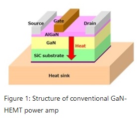
In GaN-HEMT power amps, some of the input power is converted to heat (Figure 1). This heat is dispersed into the SiC substrate, and is carried away by a cooling structure (heat sink). Although the SiC substrate has relatively high thermal conductivity, a material with even better thermal conductivity will be needed for devices with increasingly higher power output to efficiently carry device heat to the cooling structure.
Single-crystal diamond has extremely good thermal conductivity-almost five times that of a SiC substrate-and is known as a material that can efficiently spread heat. In order to bond a single-crystal diamond to a device as a cooling material, normal production processes use an Ar beam to remove impurities, which produces a low-density damaged surface that weakens the bonds the single-crystal diamond can form. Moreover, using SiN or other insulating films for bonding interferes with thermal conductivity due to SiN's thermal resistance.
About the Technology
Fujitsu and Fujitsu Laboratories have succeeded in developing the world's first technology for room-temperature bonding onto a SiC substrate single-crystal diamond, used for high-efficiency cooling of GaN-HEMT power amps. These two hard materials have different coefficients of thermal expansion (Figure 2).
To prevent the Ar beam from forming a damaged layer on the diamond surface, the companies developed a technique that protects the surface with an extremely thin metallic film before it is exposed to the Ar beam. In order to ensure the surface is planar, for good bonding at room temperature, the metallic film is held to a thickness of 10 nm or less. This technology was confirmed to prevent the formation of the damaged layer on the diamond surface after Ar beam exposure (Figure 3), resulting in improved bonding strength and single-crystal diamond bonded at room temperature to a SiC substrate for GaN-HEMT.
Figure 2: Structure of GaN-HEMT power amp with bonded diamond
Figure 3: Diamond cross section after Ar beam exposure
Figure 4: A GaN-HEMT/SiC substrate with diamond bonded using this technology
Results
Thermal resistance, which expresses how difficult it is for heat to pass through something, was measured in samples that were bonded at room temperature, and the SiC/diamond interface was found to have an extremely low thermal resistance of 6.7 x 10⁻⁸ m2K/W (square-meter kelvins per watt). Simulations using this measured parameter showed that this technology would significantly reduce thermal resistance of 200W-class devices, to 61%(5) (Figure 5). Use of this technology promises GaN-HEMT power amps for transmitters with even higher power output. When used in systems such as weather radars, GaN-HEMT power amps for transmitters could be expected to increase the radar's observable range by a factor of 1.5. This would allow for quicker detection of the cumulonimbus clouds that can produce sudden rainstorms, and contribute to a safer and more secure society in terms of disaster readiness.
Figure 5: Simulated comparison of heat in 200W-class GaN-HEMT power amps
Page 1 of 2
Share on:


Testimonial
"Our marketing partnership with I-Connect007 is already delivering. Just a day after our press release went live, we received a direct inquiry about our updated products!"
Rachael Temple - AlltematedSuggested Items
Altair, Wichita State University’s NIAR Sign MoU to Accelerate Aerospace Innovation
09/16/2025 | AltairAltair, a global leader in computational intelligence, and Wichita State University’s (WSU) National Institute for Aviation Research (NIAR), one of the world’s leading aerospace research institutions, have signed a memorandum of understanding (MoU) to advance innovation across the aerospace and defense industries.
AI-Powered Wearables Transform How Consumers Interact with Everyday Technology
09/15/2025 | PR NewswireThe global demand for AI-driven, touchless wearable technologies is accelerating as consumers seek more natural, seamless and intuitive ways to interact with their devices. Traditional touch screens and voice assistants, while effective, are increasingly viewed as limiting in a world where multitasking, mobility and efficiency are key. As industries from consumer electronics to augmented reality and enterprise computing embrace the possibilities of gesture-based control, the market for neural interfaces is rapidly expanding
Hanwha Aerospace to Collaborate with BAE Systems on Advanced Anti-jamming GPS for Guided Missiles
09/15/2025 | HanwhaHanwha Aerospace has signed a contract with BAE Systems to integrate next-generation, anti-jamming Global Positioning System (GPS) technology into Hanwha Aerospace’s Deep Strike Capability precision-guided weapon system.
United Electronics Corporation Unveils Revolutionary CIMS Galaxy 30 Automated Optical Inspection System
09/11/2025 | United Electronics CorporationUnited Electronics Corporation (UEC) today announced the launch of its new groundbreaking CIMS Galaxy 30 Automated Optical Inspection (AOI) machine, setting a new industry standard for precision electronics manufacturing quality control. The Galaxy 30, developed and manufactured by CIMS, represents a significant leap forward in inspection technology, delivering exceptional speed improvements and introducing cutting-edge artificial intelligence capabilities.
Intel Announces Key Leadership Appointments to Accelerate Innovation and Strengthen Execution
09/09/2025 | Intel CorporationIntel Corporation today announced a series of senior leadership appointments that support the company’s strategy to strengthen its core product business, build a trusted foundry, and foster a culture of engineering across the business.