-

-
News
News Highlights
- Books
Featured Books
- smt007 Magazine
Latest Issues
Current Issue
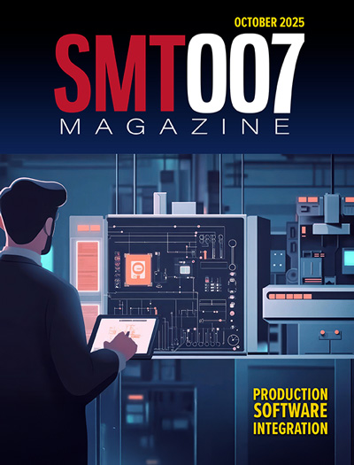
Production Software Integration
EMS companies need advanced software systems to thrive and compete. But these systems require significant effort to integrate and deploy. What is the reality, and how can we make it easier for everyone?

Spotlight on India
We invite you on a virtual tour of India’s thriving ecosystem, guided by the Global Electronics Association’s India office staff, who share their insights into the region’s growth and opportunities.

Supply Chain Strategies
A successful brand is built on strong customer relationships—anchored by a well-orchestrated supply chain at its core. This month, we look at how managing your supply chain directly influences customer perception.
- Articles
- Columns
- Links
- Media kit
||| MENU - smt007 Magazine
Tips & Tricks: Generating Stencil Tooling
December 13, 2017 | Ken Horky, Peterson ManufacturingEstimated reading time: 2 minutes
Many engineers are leaving the editing up to the stencil fabricator these days, describing the PCB array, aperture undersize/oversize, shape conversions, etc., for the fabricator to then edit. From the outside, this may appear as a time saver for all of us overworked process engineers, but considering how many stencil redos have been required and how many processes that have run “sort of OK,” there’s a tremendous amount of scrap and rework that could be saved from just a little more attention paid to stencil tooling. I prefer to make my own mistakes rather that receiving a stencil (with the project due tomorrow) and finding that someone else didn’t do something right, or misunderstood my design intent.
It’s a huge advantage for the experienced engineer to be able to produce good, first run results most, if not all, of the time. You can learn what works best for your equipment in your environment. There are several Gerber editing tools available that will let you create a library and apply changes semiautomatically or automatically to your data.
One of the most common edits used for resistors and capacitors is the “home plate” design. The left aperture below (magenta) is a typical aperture reduction. The right aperture below (cyan) is the home plate pattern. Black being the component outline and terminals, and red being the original pads.
Figure 1: Home plate design.
This is a very useful aperture design for mitigating solder balling and tombstoning. It can also be a difficult shape to describe, and convey where to apply it, to a stencil fabricator. Some large connector pins may benefit from oversizing the aperture to improve mechanical interconnect and ease inspection. Large heatsinks, such as those for DPAKs (Decawatt Package), can be divided into multiple apertures to reduce squeegee scooping and voids. Bowtie patterns can reduce solder balling on large gull wing pins.
I position the print image within my foil perimeter in the data, depending on the assembly type, and indicate the location for the stencil ID. My operators like the image forward of center for easier access, a better visual in process, and less ambiguous installation. We like to put both images of a double-sided board on the same stencil to reduce change over time. The distance between the two images needs to match your printer’s blade span and over travel distance.
Editing your own data also allows you to eliminate the check plot, further reducing your design cycle time. It also reduces the fabricator’s editing time, further improving their turn time.
Rather than spending time generating a document to describe the edits to your stencil fabricator and hoping they’ll get it right, make the edits yourself to get what you intended and improve your process.
Testimonial
"Advertising in PCB007 Magazine has been a great way to showcase our bare board testers to the right audience. The I-Connect007 team makes the process smooth and professional. We’re proud to be featured in such a trusted publication."
Klaus Koziol - atgSuggested Items
Zuken Announces ZIW Americas 2026 in Dallas
10/21/2025 | ZukenZuken USA, Inc., a global leader in electrical and electronic design automation, announced Zuken Innovation World (ZIW) Americas 2026, the company’s premier global conference dedicated to advancing the future of electrical and electronic product design. ZIW 2026 will be held June 9-11 in Dallas, Texas.
Keysight Completes Acquisition of Synopsys’ Optical Solutions Group and Ansys’ PowerArtist
10/17/2025 | Keysight Technologies, Inc.Keysight Technologies, Inc., announced the completion of its acquisitions of the Optical Solutions Group from Synopsys, Inc., and PowerArtist from Ansys, Inc.
RT-Labs Joins STMicroelectronics Partner Program to Accelerate Industrial Communication
10/16/2025 | RT-LabsRT-Labs, a leading provider of real-time software solutions for industrial automation, announces that it has joined the STMicroelectronics Partner Program to integrate its Ethernet-based industrial communication stacks into ST’s development environments and microcontroller platforms.
ASC Sunstone Circuits Adds New Options to OneQuote While Maintaining Real-Time Pricing on Core PCB Features
10/16/2025 | ASC Sunstone CircuitsASC Sunstone Circuits, a leading U.S. PCB manufacturer, today announced a significant expansion of its OneQuote online quoting tool, giving design engineers more control over complex PCB configurations — making it easier for the quote team to quickly clarify and verify specifications, reducing delays from manual quote reviews.
Analog Devices Launches ADI Power Studio™ and New Web-Based Tools
10/14/2025 | Analog Devices, Inc.Analog Devices, Inc., a global semiconductor leader, announced the launch of ADI Power Studio, a comprehensive family of products that offers advanced modeling, component recommendations and efficiency analysis with simulation. In addition, ADI is introducing early versions of two new web-based tools with a modernized user experience under the Power Studio umbrella:


