


 Knocking Down the Bone Pile: Revamp Your Components with BGA Reballing
 Global Sourcing Spotlight: Balancing Speed and Flexibility Without Sacrificing Control
 SMT Perspectives & Prospects: Artificial Intelligence Part 6: Data Module 1


Solder Printing Process Inputs Impacting Distribution of Paste Volume
December 14, 2017 | Marco Lajoie and Alain Breton, C-MAC MicroelectronicsEstimated reading time: 4 minutes
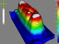
The volume of solder deposition, like any process, has variations that may be characterized by a statistical distribution curve, whether normal (from causes inherent to the process and of predictable probability) or non-normal (impacted by special causes, intermittent or inherently unpredictable). For assemblies of moderate complexity, density, cost, and reliability requirements, one may tolerate fairly large variations in volume and still obtain acceptable yields and quality of solder joints, assuming that a solder paste inspection (SPI) will effectively segregate gross defects like bridges and misalignment. Surely, this eases the task since a few hours of engineering suffice to launch a new product using standard recipes, and manufacturing may flow with minimal interruptions from SPI calls or process inputs sliding off tight windows of operation.
Why Does it Matter?
As complexity, density, cost and reliability requirements increase, there may be value in narrowing the distribution curve. It is common sense that less variation serves the interest of quality of the more complex and dense circuit boards. It can also affect the cost as it should increase the yield and reduce rework and scrap. It does this by reducing the normal variations but also by revealing the outliers, driven by identifiable special causes which, otherwise, would have remained hidden in larger acceptance windows.
Reliability is typically assessed by tests performed on relatively small sample size of products from a limited number of lots, sometimes repeated at relatively long intervals. In other words, how much of the actual distribution was represented in the samples tested and how different are the parts produced between test intervals? Narrower distribution should help ensure reproducibility of reliability performance across test samples and production units alike.
What Target?
Common sense dictates that narrower is better. But how narrow is enough? A typical industry target for solder joint quality is IPC-610, with subclasses 1 to 3. Performing a simple DOE, one would find that most IPC criteria can be met across a fairly large distribution of solder volumes. However, mere compliance to IPC may not meet expectations when confronted with the subtle causes of defect modes like tombstones, voiding in thermal planes, or open corner balls of BGA. Besides, IPC criteria defining ranges of acceptable solder volume from "wetting is evident" to "solder shall not touch a package body" hardly sounds like a valid predictor of product reliability under harsh conditions.
In other words, you are left with the task of identifying the weak spots: your highest pareto causes in yields, your first fail modes to occur in highly accelerated life testing (HALT) or other test-to-fail methodology. Then, identify best nominal targets and narrow distribution for each, most of the time iteratively until you consider having reached stability. This is lots of work, far from the ease of using standard recipes. With experience and methodology, patterns and targets get more predictable, and the investments start paying off.
What Process Inputs?
In search of better performance criteria (e.g., yield, reliability…) once you suspect that distribution of solder volume is a significant contributor, what process inputs may impact your distribution? Consider the 6M classification: measurement, machine, material, mother nature, method, manpower.
Measurement
"Know thy SPI" might say the Greek philosopher Thales, if assigned to the task. Measurement starts with proper measurement system analysis (MSA), which includes calibration and Gage repeatability and reproducibility (R&R). However, wet solder paste samples may not remain sufficiently stable through the course of the analysis. Options include, for calibration: a 3D reference of a known volume, traceable to international standards; for Gage R&R: dried (long stabilized) paste, with care to present samples across the entire range of measurements.
Additionally, SPI measurements may include various artifacts originating from: incorrect reference plane (referencing to solder resist instead of copper), PCB warping, shadowing from adjacent solder depositions, etc. The most recent generations of SPI include specific features to address these. Chances are that these are minor and only impact the few measurements that are so critical in your application. The point is to understand the limitations of your measurements, so their variations are not confused with other process inputs, or lead you to wrong conclusions.
Make measurement part of a formal control plan (i.e., who, what, when, how is the process measured, under what control limits, and what reaction is expected if out of range). Include technical management as part of reaction plans to first-time quality (FTQ) or SPC signals, so they can intervene in close time and proximity while the trail is hot, and continuously improve the process.
Machine
Machine includes process equipment and tooling. Assuming programming and maintenance are executed thoroughly, printers are usually stable for the purpose unless anomalies went undetected, like: planarity of stencil mounting, measurement from the load cell (pressure), squeegee mounting, etc.
As for tooling, ask your supplier for the tolerances of your stencil. On a given unit, variations in thickness and apertures alone may cause significant variations between circuits across the same panel. Similarly, ordering a new stencil from the same image may not yield the same results. Also, the limits and trends of the tolerances may differ between fabrication methods (laser cut, electroformed, nanocoated, etc.). Finally, consider its maintenance plan: How efficient is cleaning after use? At what frequency and under what criteria is it evaluated for reuse?
Squeegees are also a key variable for solder deposition. Include blade material (metal or polyurethane) and maintenance protocol (wear, cleanliness) in your potential variables.
Finally, board support matters, with a solid block yielding the most repeatable results. Obviously, printing on second side forces to trade support for component clearance and strategies differ: blocks with custom cavities, grid-patterned automated posts, or manually placed posts. Some PCB designs and types (thin, oddshape, flex…) may require process carriers whose design (planarity, clamping) are of prime importance.
To read the full version of this article, which appeared in the November 2017 issue of SMT Magazine, click here.
Share on:


Testimonial
"Our marketing partnership with I-Connect007 is already delivering. Just a day after our press release went live, we received a direct inquiry about our updated products!"
Rachael Temple - AlltematedSuggested Items
Rehm Wins Mexico Technology Award for CondensoXLine with Formic Acid
10/17/2025 | Rehm Thermal SystemsModern electronics manufacturing requires technologies with high reliability. By using formic acid in convection, condensation, and contact soldering, Rehm Thermal Systems’ equipment ensures reliable, void-free solder joints — even when using flux-free solder pastes.
Indium Experts to Deliver Technical Presentations at SMTA International
10/14/2025 | Indium CorporationAs one of the leading materials providers to the power electronics assembly industry, Indium Corporation experts will share their technical insight on a wide range of innovative solder solutions at SMTA International (SMTAI), to be held October 19-23 in Rosemont, Illinois.
Knocking Down the Bone Pile: Revamp Your Components with BGA Reballing
10/14/2025 | Nash Bell -- Column: Knocking Down the Bone PileBall grid array (BGA) components evolved from pin grid array (PGA) devices, carrying over many of the same electrical benefits while introducing a more compact and efficient interconnect format. Instead of discrete leads, BGAs rely on solder balls on the underside of the package to connect to the PCB. In some advanced designs, solder balls are on both the PCB and the BGA package. In stacked configurations, such as package-on-package (PoP), these solder balls also interconnect multiple packages, enabling higher functionality in a smaller footprint.
Indium to Showcase High-Reliability Solder and Flux-Cored Wire Solutions at SMTA International
10/09/2025 | Indium CorporationAs one of the leading materials providers in the electronics industry, Indium Corporation® will feature its innovative, high-reliability solder and flux-cored wire products at SMTA International (SMTAI), to be held October 19-23 in Rosemont, Illinois.
‘Create your Connections’ – Rehm at productronica 2025 in Munich
10/08/2025 | Rehm Thermal SystemsThe electronics industry is undergoing dynamic transformation: smart production lines, sustainability, artificial intelligence, and sensor technologies dominate current discussions.