


 SMT Perspectives & Prospects: The Architecture of Winston Churchill’s Leadership
 Global Sourcing Spotlight: Making Global Sourcing Simple Again
 The Government Circuit: New Council Now Helps Shape Policy Decisions in the Electronics Supply Chain


The ongoing miniaturization trend in the SMT production induces new challenges and highly integrated systems. In passive components, the miniaturization leads to the introduction of the EIA size 01005 or smaller. Typical 01005 components are chip resistors and chip capacitors with the dimension of 0.4 mm x 0.2 mm. Despite numerous publications in this field already addressing the printing of such devices, a defined wholly optimized process remains unsolved and inspires further novel research ideas on this topic.
This paper focuses on the stencil printing process, because the highest amount of failure is assumed to be based on this process step. Furthermore, the paper extends the preliminary work by fundamental considerations. Thereby different values for the area ratio will be part of the investigation, which are purposely set to very low limits.
The influence of the aperture shape and orientation on the solder printing performance will be discussed. It is based on different forms of rectangles. Starting with a square the dimensions are incrementally changed, so that the square converts further into a rectangle. Furthermore, each rectangle is additionally rotated by 90° to be able to evaluate the influence of the apertures direction towards the squeegee.
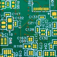
Figure 1: PCB and solder paste deposit layout.
In addition to the previously described stencil aperture attributes, this research also explores different stencil thicknesses, solder pastes and a variation of the squeegee speed. The evaluation of all data will be based on the two criteria of transfer efficiency and standard deviation. For both experiments the same stencil layouts and same solder paste are being used. The paper concludes with an outlook and suggestions on the modification of the current calculation by limitations of aperture dimensions.
Experimental Setup
The experimental setup includes three main variables, namely the layout by the PCB, the solder paste and the stencils used. A description of the experiment process is further explained.
PCB Layout
For the stencil printing experiments, a black anodized aluminum plate is used as substrate material with dimensions of 160 x 160 x 1.5 mm. This material is highly rigid and planar, representing a near perfect printing surface to minimize its influence on the print process outcome. Furthermore, the black aluminum material enables higher contrasts at the SPI, leading to more precise measurements. Figure 1 shows the general design of the printed solder paste deposits on the PCB.
Solder Paste
The stencil printing test also aimed to compare four different no-clean SAC305 solder paste formulations varying by type and by manufacturer. Solder paste of type 4 and type 5 were used. By the IPC J-STD-005 at least 80% of the alloy powder in a type 4 paste measures 20-38 μm while a type 5 paste contains the same ratio of alloy in 15-25 μm diameter particles. Due to the small dimensions of the tested apertures a difference in the printing performance attributed to particle size (i.e., type) is assumed a reasonable possibility. Two paste vendor sources were also included in this study, named A and B, which were supplied in both type 4 and type 5 products. As the distribution of the solder paste particles is comparable, A and B mainly differ in the composition of their flux systems which affects rheology and printing capability.
Stencils
In total three stencils were used for the experiments. Firstly, the stencils differ by their thickness and secondly by the size of their apertures (compare Table 1 to Table 3). The general structure is identical. The layout (Figure 1) can be divided into rows and columns. Each row represents an area ratio, starting in Row A with AR of 0.45 and ending with AR of 0.65 in Row E. Each column in these tables represents different aperture shapes. Column 1 always has the shape of a circle, Column 7 is a square and Column 13 is the form of a diamond. Column 14 contains special types of structures that will not be discussed in this paper. Columns 2-6 and 8-12 are paired with the same dimensions and they only differ in their orientation towards the squeegee. Columns 2-6 face with the small side the squeegee (i.e., north-south orientation), whereby columns 8-12 face the squeegee with the long side of the rectangle (east-west orientation).
To read the full version of this article, which appeared in the December 2017 issue of SMT Magazine, click here.


