


 Nolan’s Notes: Our Spotlight on North America
 Global Sourcing Spotlight: Building a Supply Chain That Bends, Not Breaks
 Smart Automation: The Journey of a Component Through an SMT Factory
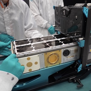


Selecting X-Ray Inspection Equipment
January 24, 2018 | Russell Poppe, JJS ManufacturingEstimated reading time: 6 minutes

There is a continuing trend towards smaller, more densely-populated printed circuit board (PCB) assemblies in electronics manufacturing. This is not necessarily because the PCB assembly needs to be smaller, but new designs are using significantly more ball grid array (BGA) and other types of devices with hidden solder connections, such as quad flat no-leads (QFN) and land grid arrays (LGAs). Such devices often have performance and cost advantages over larger packages with leads, so the trend is likely to continue.
Automated optical inspection (AOI) is an established, key process control in the SMT industry that greatly increases confidence in the quality of the finished product. But what do you do about devices where you cannot optically see the solder connections? X-ray inspection provides the answer.
Using X-ray as an in-process control can help remove the risk of producing assemblies that are impossible or uneconomical to repair due to misplaced ‘hidden connection’ devices. Reworking a misplaced device can be time consuming and may cause other issues on the assembly, for example with surrounding components on the PCB due to local heating. Rework might also exceed the maximum number of solder reflow cycles allowed for double-sided assemblies. Finding a failure later in the process, for example at JTAG or functional test, incurs additional lost time and cost in diagnosis and re-test.
So, when should you use X-ray? It should certainly be part of the ‘first-off’ inspection process, helping to ensure the oven profile is optimal for the leadless devices. It might then be sensible to check a sample of assemblies as they go through production; a few from the start, middle and end of the batch is typical. Alternatively, an ‘in line’ process might be used, though it is worth noting that X-ray inspection—even if automated—is relatively slow. In practice, placing leadless devices, especially BGAs, is quite straightforward and normally causes few issues, so X-ray should be employed thoughtfully.
Figure 1: X-ray allows inspection without resorting to potentially destructive re-work or micro-sectioning.
X-ray inspection can also help reduce end-of-line manual inspection, for example on fine-pitch devices that cannot be fully covered by AOI (depending on what type of system you have), or where other BGA inspection methods such as an Ersascope might have been used. Another great benefit of X-ray inspection is in resolving quality issues. X-ray allows inspection without resorting to potentially destructive re-work or micro sectioning, which adds cost and, of course, leads to a scrapped assembly. Micro-sectioning also requires a bit of an educated guess as to where the problem might be.
How often have your heard someone say, “It fails test, it doesn’t work, and I can’t see where the problem is, so it must be the BGA”? Enhancing X-ray to provide laminography, or indeed, full 3D capability that enables the inspector to walk through an assembly, helps find faults such as broken tracks or barrels in a PCB, for example, as well as any issues with leadless components.
Away from PCBAs, X-ray can provide nondestructive inspection of other manufactured components such as cable assemblies or machined parts where there is a need to see interior detail. It can also provide a degree of measurement capability.
So, a capable X-ray inspection facility is now considered a must-have for modern electronics assembly lines. But now that you have decided you need one yourself, or that your electronics manufacturing services (EMS) partner should be investing on your behalf, how do you go about choosing the right system?
Key Considerations
There are a lot of vendors and systems out there, so as with all capital equipment evaluations it is best to start looking with a must-have list already in mind. We will assume that price (and payback) will be part of the equation, and of course, the system must be large enough to accommodate the items that you want to inspect.
The following are four more areas to consider:
1. Image quality
If you were looking to buy a camera, then one with a higher pixel count, say, 24MP, is better quality than one with 16MP, right? If you know a bit about photography, you will know this is a great over-simplification (if not just plain nonsense), and if anything, X-ray can seem even more complicated.
There are physics and very clever software involved. Things that can affect image quality include the power, voltage, spot size, detector resolution, proximity of the X-ray source to the item and the field of view. Take voltage, for example. A 160kV system will have greater X-ray penetration capability than say a 130kV system, but the higher voltage can adversely affect the image contrast and hence, quality. How do you decide? The most practical solution is to take some typical sample assemblies and try the X-ray system out. Image quality can be a subjective opinion.
The great news is that you will probably find that systems aimed at PCB assemblies provide image quality that ranges from very good to excellent. This can perhaps be more to do with how the inspection is set up than the technical capability of its components.
Page 1 of 2
Share on:


Testimonial
"In a year when every marketing dollar mattered, I chose to keep I-Connect007 in our 2025 plan. Their commitment to high-quality, insightful content aligns with Koh Young’s values and helps readers navigate a changing industry. "
Brent Fischthal - Koh YoungSuggested Items
Indium to Showcase High-Performance AI Application Solutions at SEMICON SEA 2026
05/01/2026 | Indium CorporationAs a leading provider of advanced materials solutions for today’s demanding AI applications, Indium Corporation® will feature its high-reliability product portfolio at SEMICON SEA 2026, May 5-7, in Kuala Lumpur, Malaysia.
ACCM Unveils Negative and Near-zero CTE Materials for Large-Format AI Chips
04/21/2026 | Advanced Chip and Circuit MaterialsAdvanced Chip and Circuit Materials, Inc. (ACCM) has launched two new materials: Celeritas HM50, with a negative coefficient of thermal expansion (CTE) of -8 ppm/°C to offset the positive CTE and expansion of copper with temperature on circuit boards, and Celeritas HM001, with near-zero CTE and the low-loss performance needed for high-speed signal layers to 224 Gb/s and faster in artificial intelligence (AI) circuits.
SMTA Ultra HDI Symposium, Day 2: Fragile Supply Chains, Fierce Innovation
04/14/2026 | Marcy LaRont, I-Connect007The Arizona weather yielded another beautiful day as we gathered for the second day of SMTA’s annual UHDI symposium. After the first full day discussing the role of AI in business and the how-tos of implementation, Avondale Mayor Mike Pineda kicked off day two, proud to showcase his city and to declare its important place in the continued development of the West Valley, an increasingly important area for tech and manufacturing.
KYZEN Focuses on Aqueous and Stencil Cleaning Solutions at SMTA Monterrey Expo and Tech Forum
04/10/2026 | KYZEN'KYZEN, the global leader in innovative environmentally friendly cleaning chemistries, will exhibit at the SMTA Monterrey Expo & Tech Forum.
Solder Paste Innovations for Enhanced Reliability from MacDermid Alpha Electronics Solutions
04/10/2026 | Real Time with... APEX EXPOJason Fullerton of MacDermid Alpha Electronics Solutions discusses innovative alloys like Innolot MXE, low-temperature solder options, and polymer reinforcement strategies. Learn how these solutions address the growing demands of high-performance computing and larger component assemblies, ensuring optimal performance and cost-effectiveness.