


 Knocking Down the Bone Pile: The Business Case for Component Reclamation
 Global Sourcing Spotlight: The Hidden Power of the Rep Network
 Smart Automation: When Traditional Depaneling Methods Reach Their Limits


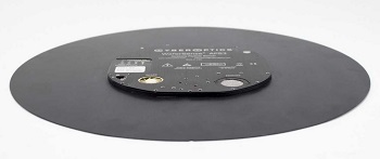
CyberOptics Corporationnannounces it will demonstrate its next generation Airborne Particle Sensor technology (APS3) 300mm with new ParticleSpectrum software at SEMICON Korea, January 31st through February 2nd at the Seoul COEX in booth # A418.
CyberOptics’ WaferSense APS3 speeds equipment set-up and long-term yields in semiconductor fabs by wirelessly detecting, identifying and monitoring airborne particles in real-time. CyberOptics’ Airborne Particle Sensors, documented as the best known method (BKM), have proven to deliver up to 90% timesavings, 95% expense reduction and up to 20X the throughput with half the manpower relative to legacy surface scan wafer methods.
The APS3 measurement devices are even thinner and lighter to travel through semiconductor tools with ease, while providing the industry-leading accuracy and sensitivity valued by equipment and process engineers around the world. The APS3 solution incorporates ParticleSpectrum software – a completely new, touch-enabled interface with user-friendly functionality, making it simple to read in real-time, record and review small to large airborne particle data.
“Semiconductor fabs and equipment OEMs worldwide have relied on our proven airborne particle sensing technology to provide significant improvements in yields,” said Dr. Subodh Kulkarni, President and CEO, CyberOptics. “Now, we’ve made the device even thinner and lighter and combined it with ParticleSpectrum, a software package that is sure to delight the engineers with its simplicity.”
At SEMICON Korea, CyberOptics will also unveil a new Airborne Particle Sensor designed for the Flat Panel Display (FPD) market.
About the WaferSense and ReticleSense Line
The WaferSense measurement portfolio including the Auto Leveling System (ALS), the Auto Gapping System (AGS), the Auto Vibration System (AVS), the Auto Teaching System (ATS), the Airborne Particle Sensors and the new Auto Multi Sensor (AMS), are available in various wafer shaped form factors depending on the device, including 150mm, 200mm and 300mm wafer sizes. The ReticleSense measurement portfolio including the Airborne Particle Sensors (APSR & APSRQ), the Auto Leveling System (ALSR) and the Auto Multi Sensor (AMSR) are available in a reticle shaped form factor.
About CyberOptics
CyberOptics Corporation is a leading global developer and manufacturer of high precision sensing technology solutions. CyberOptics sensors are being used in general purpose metrology and 3D scanning, surface mount technology (SMT) and semiconductor markets to significantly improve yields and productivity. By leveraging its leading edge technologies, the company has strategically established itself as a global leader in high precision 3D sensors, allowing CyberOptics to further increase its penetration of its key vertical segments. Headquartered in Minneapolis, Minnesota, CyberOptics conducts worldwide operations through its facilities in North America, Asia and Europe. For more information about the entire line of CyberOptics solutions please click here.


