


 Marcy’s Musings: From Pitch to PO—The Sales Stack
 It’s Only Common Sense: Knowing When to Walk Away
 Dan’s Biz Bookshelf: ‘Elevate: Push Beyond Your Limits'


Plasmatreat North America Names Hardev Grewal New CEO
February 15, 2018 | Plasmatreat North AmericaEstimated reading time: 1 minute
Effective January 2018, Hardev Grewal has assumed the position of President & CEO of Plasmatreat North America.
Hardev Grewal was born in Munich, Germany. As the son of an Indian father, a semiconductor R&D scientist at Siemens, and a German mother, he started his international career while getting his degree in industrial engineering and business administration at the University of Applied Science Munich with a six month stint in India working for technology conglomerate ABB. Two years later he accepted an opportunity to co-op in California with semiconductor giant Applied Materials. Realizing Grewal's business acumen, the company sponsored his research work and recruited him to permanently join them in Silicon Valley where he quickly advanced his career to Director of Global Product Management.
After 16 years in the semiconductor industry, Grewal joined the M+W Group in 2010 to grow their newly acquired subsidiary NSTAR Global Services with developing new product and service solutions. Soon thereafter he was promoted to Vice President, Global Sales and Business Operations.
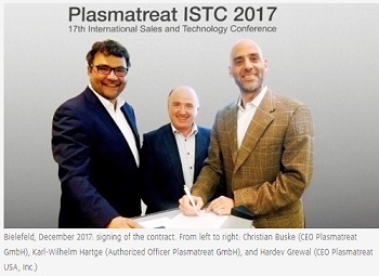
In joining Plasmatreat, Hardev Grewal continues his presence in Silicon Valley. The company has recently built its largest and most advanced technology center in Hayward, CA. The newly appointed leader of the North American team is quite familiar with plasma. "I have been exposed to the technology since my early childhood," he says, laughing. "My father has been a leading scientist with many patents in the low pressure plasma technology for semiconductor devices."
The fact that the son now deals with hi-tech atmospheric plasma jets instead of vacuum chambers is a welcomed new challenge. "The potential for using atmospheric plasma technology in many different industries is nearly unlimited," Grewal states enthusiastically. "Combined with a strong and knowledgeable team that I look forward to working with, we will not only hold, but expand our market leadership position in the Americas."
Outside of work, the 47-year-old industrial engineer enjoys a variety of things centered around food and sports. "I love to cook, enjoy good food and am a passionate cyclist - both road and mountain - preferably with my 15 year old son, whose high school team I also coach." The Plasmatreat Group cordially welcomes their new colleague, wishing him speed, endurance and lots of success with his sports and business activities.
Share on:


Suggested Items
Microchip Enters into Partnership Agreement with Delta Electronics on Silicon Carbide Solutions
07/18/2025 | Globe NewswireThe growth of artificial intelligence (AI) and the electrification of everything are driving an ever-increasing demand for higher levels of power efficiency and reliability.
ViTrox’s HITS 5.0 Empowers Global Partners with Innovative Solutions and Stronger Bonds
07/16/2025 | ViTroxViTrox, strives to be the World’s Most Trusted Technology Company, proudly announces the successful conclusion of its fifth edition of High Impact Training for Sales (HITS 5.0), held from 23rd to 27th June 2025 at ViTrox Campus 2.0 and 3.0, located in Batu Kawan Industrial Park, Penang, Malaysia.
Global Citizenship: The Global Push for Digital Inclusion
07/16/2025 | Tom Yang -- Column: Global CitizenshipIt can be too easy to take the technology at our fingertips for granted: high-speed internet, cloud-based collaboration, and instant video calls across continents. Yet, for billions of people, access to these digital tools is a distant dream. As a global community, we must ensure that technology is available to all. Here is how technology is bridging physical, economic, and educational gaps in underserved regions and profoundly reshaping lives.
Microchip Expands Space-Qualified FPGA Portfolio with New RT PolarFire® Device Qualifications and SoC Availability
07/10/2025 | MicrochipContinuing to support the evolving needs of space system developers, Microchip Technology has announced two new milestones for its Radiation-Tolerant (RT) PolarFire® technology: MIL-STD-883 Class B and QML Class Q qualification of the RT PolarFire RTPF500ZT FPGA and availability of engineering samples for the RT PolarFire System-on-Chip (SoC) FPGA.
Infineon Advances on 300-millimeter GaN Manufacturing Roadmap as Leading Integrated Device Manufacturer (IDM)
07/10/2025 | InfineonAs the demand for gallium nitride (GaN) semiconductors continues to grow, Infineon Technologies AG is poised to capitalize on this trend and solidify its position as a leading Integrated Device Manufacturer (IDM) in the GaN market.