


 Dan’s Biz Bookshelf: ‘The Next RenAIssance: AI and the Expansion of Human Potential’
 The Chemical Connection: When the Industry Moves Faster Than the Standards
 Driving Innovation: Selecting the Right Laser Source


Materials 'Sandwich' Breaks Barrier for Solar Cell Efficiency
March 15, 2018 | New York University Tandon School of EngineeringEstimated reading time: 4 minutes
Solar cells have great potential as a source of clean electrical energy, but so far they have not been cheap, light, and flexible enough for widespread use. Now a team of researchers led by Tandon Associate Professor André D. Taylor of the Chemical and Biomolecular Engineering Department has found an innovative and promising way to improve solar cells and make their use in many applications more likely.
Most organic solar cells use fullerenes, spherical molecules of carbon. The problem, explains Taylor, is that fullerenes are expensive and don’t absorb enough light. Over the last 10 years he has made significant progress in improving organic solar cells, and he has recently focused on using non-fullerenes, which until now have been inefficient. However, he says, “the non-fullerenes are improving enough to give fullerenes a run for their money.”
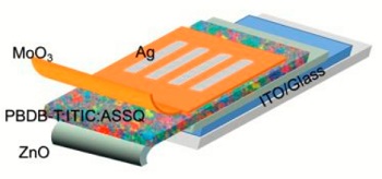
Think of a solar cell as a sandwich, Taylor says. The “meat” or active layer — made of electron donors and acceptors — is in the middle, absorbing sunlight and transforming it into electricity (electrons and holes), while the “bread,” or outside layers, consist of electrodes that transport that electricity. His team’s goal was to have the cell absorb light across as large a spectrum as possible using a variety of materials, yet at the same time allow these materials to work together well. “My group works on key parts of the ‘sandwich,’ such as the electron and hole transporting layers of the ‘bread,’ while other groups may work only on the ‘meat’ or interlayer materials. The question is: How do you get them to play together? The right blend of these disparate materials is extremely difficult to achieve.”
The research team led by André Taylor, working with the active layer of an organic solar cell, achieved remarkable efficiency by introducing a squarine molecule (ASSQ) as a crystallizing agent, which both donates electrons and enhances the light absorption of the active layer of the cell, properly orienting the PBDB-T donor-acceptor polymer that accepts the donor electron with the with the non-fullerene electron-acceptor molecule ITIC.
Using a squaraine molecule in a new way — as a crystallizing agent — did the trick. “We added a small molecule that functions as an electron donor by itself and enhances the absorption of the active layer,” Taylor explains. “By adding this small molecule, it facilitates the orientation of the donor-acceptor polymer (called PBDB-T) with the non-fullerene acceptor, ITIC, in a favorable arrangement.”
This solar architecture also uses another design mechanism that the Taylor group pioneered known as a FRET-based solar cell. FRET, or Förster resonance energy transfer, is an energy transfer mechanism first observed in photosynthesis, by which plants use sunlight. Using a new polymer and non-fullerene blend with squaraine, the team converted more than 10% of solar energy into power. Just a few years ago this was considered too lofty a goal for single-junction polymer solar cells. "There are now newer polymer non-fullerene systems that can perform above 13%, so we view our contribution as a viable strategy for improving these systems," Taylor says.
The organic solar cells developed by his team are flexible and could one day be used in applications supporting electric vehicles, wearable electronics, or backpacks to charge cell phones. Eventually, they could contribute significantly to the supply of electric power. “We expect that this crystallizing-agent method will attract attention from chemists and materials scientists affiliated with organic electronics,” says Yifan Zheng, Taylor’s former research student and lead author of the article about the work in the journal Materials Today.
Next for the research team? They are working on a type of solar cell called a perovskite as well as continuing to improve non-fullerene organic solar cells.
“A Highly Efficient Polymer Non-Fullerene Organic Solar Cell Enhanced by Introducing a Small Molecule as a Crystallizing-Agent” is available at ScienceDirect.
In addition to Taylor and Zheng, co-authors are Jiang Huang and Junsheng Yu of the University of Electronic Science and Technology of China; Gang Wang of Northwestern University; Jaemin Kong, a post-doctoral researcher now at NYU; and Di Huang, Megan Mohadjer Beromi, and Nilay Hazari of Yale. The National Natural Science Foundation of China, the Project of Science and Technology of Sichuan Province, the U.S. National Science Foundation, and the Yale Institute for Nanoscience and Quantum Engineering supported the research.
About the New York University Tandon School of Engineering
The NYU Tandon School of Engineering dates to 1854, the founding date for both the New York University School of Civil Engineering and Architecture and the Brooklyn Collegiate and Polytechnic Institute (widely known as Brooklyn Poly). A January 2014 merger created a comprehensive school of education and research in engineering and applied sciences, rooted in a tradition of invention and entrepreneurship and dedicated to furthering technology in service to society. In addition to its main location in Brooklyn, NYU Tandon collaborates with other schools within NYU, the country’s largest private research university, and is closely connected to engineering programs at NYU Abu Dhabi and NYU Shanghai. It operates Future Labs focused on start-up businesses in downtown Manhattan and Brooklyn and an award-winning online graduate program. For more information, click here.
Share on:


Subscribe
Stay ahead of the technologies shaping the future of electronics with our latest newsletter, Advanced Electronics Packaging Digest. Get expert insights on advanced packaging, materials, and system-level innovation, delivered straight to your inbox.Subscribe now to stay informed, competitive, and connected.
Suggested Items
I-Connect007 Editor’s Choice: Five Must-Reads for the Week
05/01/2026 | Michelle Te, I-Connect007If it feels like the PCB industry is accelerating faster than ever, you’re not imagining it. From advanced materials driven by AI applications to renewed investment in domestic manufacturing—and the next generation stepping into critical roles—there’s a lot shifting at once. My selections for this week highlight where the pressure points are forming, and where the opportunities are emerging.
Electronics Manufacturing Needs Your Voice: Global Sentiment Survey Now Live
04/30/2026 | Global Electronics AssociationThe latest monthly Global Sentiment Survey from the Global Electronics Association is now open. At a time when demand uncertainty, policy shifts, energy costs, and supply chain recalibration are pulling the industry in multiple directions, the survey captures something macroeconomic data often misses: how manufacturers are actually experiencing conditions on the ground.
From Backbone to Breakthroughs: I-Connect007 Wraps PCB Materials Series with Focus on Innovation
04/30/2026 | I-Connect007I-Connect007 wraps up its six-part podcast series, PCB Materials: The Backbone and Future of Electronics, with Episode 6 and a discussion focusing on innovation. In Episode 6, Marcy LaRont speaks with Isola CTO Kirk Thompson about a critical turning point for the PCB industry as innovation accelerates. As data rates climb and demands from AI infrastructure, power density, flexible electronics, photonics, and chiplet integration intensify, traditional material assumptions are no longer sufficient.
Jiva Soluboard Getting the Attention It Deserves
04/30/2026 | Marcy LaRont, I-Connect007 MagazineJiva is a newer company that bridges the divide between PCB fabrication and product circularity or sustainability. Jiva Soluboard is the first fully recyclable laminate material ever created for PCB fabrication, and it's not going unnoticed. Stephen Driver, CEO of Jiva, gave us an update at APEX EXPO, including an exciting certification achievement in February.
Driving Innovation: Selecting the Right Laser Source
04/28/2026 | Simon Khesin -- Column: Driving InnovationWhen I first joined Schmoll Maschinen, I brought experience from almost every PCB process, except for laser. As I immersed myself in laser processing, I realized why it can seem so daunting to a newcomer. The complexity arises from three intersecting factors: A vast variety of laser sources: CO2, UV-nano, green-pico, UV-pico, IR-pico, and others; a diverse range of applications: Drilling, cutting, ablation, and more; and an extensive list of materials: These have vastly different absorption rates. Choosing the right machine or laser source is rarely trivial. Even for experienced engineers, answering "Which source is best?" requires examining the business's specific goals.