


 Dan’s Biz Bookshelf: ‘The Next RenAIssance: AI and the Expansion of Human Potential’
 The Chemical Connection: When the Industry Moves Faster Than the Standards
 Driving Innovation: Selecting the Right Laser Source


A New Way to Atomically Thin Materials
April 5, 2018 | WileyEstimated reading time: 2 minutes
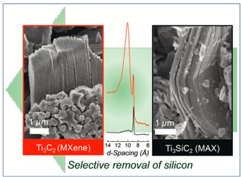
Metallic conductivity and hydrophilicity of MXenes have established them as electrodes in rechargeable batteries and supercapacitors, as well as other applications, including photothermal cancer therapy, electromagnetic shielding, water purification and gas sensing. In the journal Angewandte Chemie, researchers have now introduced a new production method. Instead of using conventional, yet more expensive, titanium aluminum carbide, they selectively etch silicon out of titanium silicon carbide, a cheaper and more common precursor, to synthesize titanium carbide.
Two-dimensional materials, consisting of extremely thin layers that are a few atoms thick, have unique properties that are completely different than the normal three-dimensional versions. A prominent example of this is graphene, which is made of single layers of carbon atoms. In 2011, a new class of two-dimensional materials was synthesized at Drexel University in Philadelphia (Pennsylvania, USA). Known as MXenes, the materials are made of transition metal carbides and nitrides, where the M stands for a transition metal, such as titanium, vanadium, or molybdenum, X can be carbon and/or nitrogen, and many compositions are available (about 30 have already been experimentally demonstrated and dozens more are expected). One such MXene is titanium carbide, Ti3C2.
Obtaining the desired MXene usually involves a roundabout process: Layered carbides and nitrides, known as MAX phases, are selectively etched with hydrofluoric acid to remove the layers of the “A” element, which is a group 13 or 14 element such as aluminum, silicon, or germanium. In this way, titanium carbide can be obtained by etching the aluminum out of titanium aluminum carbide (Ti3AlC2). However, this starting material is expensive, and the production is complex. In contrast, the silicon analog, titanium silicon carbide (Ti3SiC2), is commercially available and less expensive. Ti3SiC2 was the first MAX phase Drexel researchers tried to selectively etch in 2011, but synthesis failed using hydrofluoric acid alone because the silicon atoms are strongly bound to the adjacent transition metal atoms.
A team led by Yury Gogotsi at Drexel University has now developed a successful variation of this process. By adding an oxidizing agent, the researchers could weaken the silicon bonds and oxidize silicon. Using mixtures of hydrofluoric acid and an oxidizing agent like nitric acid, hydrogen peroxide, or potassium permanganate, the team produced titanium carbide MXene by selectively removing silicon out of Ti3SiC2.
The etching process leaves behind stacks of titanium carbide, which can be delaminated to make flakes, which are approximately 1 nanometer in thickness. The researchers used this method to make flexible, electrically conducting titanium carbide films on a relatively large scale.
This new method could make the production of MXenes easier, and open pathways to the production of new MXenes and related two-dimensional materials from silicon-containing precursors, expanding the family of 2D nanosheets available to scientists and engineers.
Share on:


Subscribe
Stay ahead of the technologies shaping the future of electronics with our latest newsletter, Advanced Electronics Packaging Digest. Get expert insights on advanced packaging, materials, and system-level innovation, delivered straight to your inbox.Subscribe now to stay informed, competitive, and connected.
Suggested Items
I-Connect007 Editor’s Choice: Five Must-Reads for the Week
05/01/2026 | Michelle Te, I-Connect007If it feels like the PCB industry is accelerating faster than ever, you’re not imagining it. From advanced materials driven by AI applications to renewed investment in domestic manufacturing—and the next generation stepping into critical roles—there’s a lot shifting at once. My selections for this week highlight where the pressure points are forming, and where the opportunities are emerging.
Electronics Manufacturing Needs Your Voice: Global Sentiment Survey Now Live
04/30/2026 | Global Electronics AssociationThe latest monthly Global Sentiment Survey from the Global Electronics Association is now open. At a time when demand uncertainty, policy shifts, energy costs, and supply chain recalibration are pulling the industry in multiple directions, the survey captures something macroeconomic data often misses: how manufacturers are actually experiencing conditions on the ground.
From Backbone to Breakthroughs: I-Connect007 Wraps PCB Materials Series with Focus on Innovation
04/30/2026 | I-Connect007I-Connect007 wraps up its six-part podcast series, PCB Materials: The Backbone and Future of Electronics, with Episode 6 and a discussion focusing on innovation. In Episode 6, Marcy LaRont speaks with Isola CTO Kirk Thompson about a critical turning point for the PCB industry as innovation accelerates. As data rates climb and demands from AI infrastructure, power density, flexible electronics, photonics, and chiplet integration intensify, traditional material assumptions are no longer sufficient.
Jiva Soluboard Getting the Attention It Deserves
04/30/2026 | Marcy LaRont, I-Connect007 MagazineJiva is a newer company that bridges the divide between PCB fabrication and product circularity or sustainability. Jiva Soluboard is the first fully recyclable laminate material ever created for PCB fabrication, and it's not going unnoticed. Stephen Driver, CEO of Jiva, gave us an update at APEX EXPO, including an exciting certification achievement in February.
Driving Innovation: Selecting the Right Laser Source
04/28/2026 | Simon Khesin -- Column: Driving InnovationWhen I first joined Schmoll Maschinen, I brought experience from almost every PCB process, except for laser. As I immersed myself in laser processing, I realized why it can seem so daunting to a newcomer. The complexity arises from three intersecting factors: A vast variety of laser sources: CO2, UV-nano, green-pico, UV-pico, IR-pico, and others; a diverse range of applications: Drilling, cutting, ablation, and more; and an extensive list of materials: These have vastly different absorption rates. Choosing the right machine or laser source is rarely trivial. Even for experienced engineers, answering "Which source is best?" requires examining the business's specific goals.