


 It’s Only Common Sense: Create Passion That Customers Feel
 Punching Out: How to Stay Focused in Business and M&A


NIST researchers have pioneered a process that drastically simplifies fabrication of the kind of nanoscale microchip features that may soon form the basis of a quantum computer, among other applications.
Instead of conventional 1-or-0 computer bits stored in the form of electrical charges, quantum information is stored and manipulated in the form of quantum bits (qubits), which can have multiple values simultaneously. One highly promising qubit candidate is a single atom of elements such as phosphorus (P) buried in ultra-pure silicon-28.
These atoms can be precisely placed using a scanning tunneling microscope (STM), a workhorse laboratory instrument widely available to scientists who may not have access to other complex nanofabrication tools.
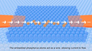
To create a nanowire, a silicon lattice is first coveredwith a layer of hydrogen atoms. A scanning electron microscope (SEM) removes asection of hydrogen, exposing the silicon beneath. A stream of phosphine gas isdirected onto the surface, leaving phosphine molecules bonded to the exposedsilicon. The lattice is then baked, removing the hydrogen layer and embeddingthe phosphorus into the silicon. Finally, additional silicon layers are addedon top.
Using an STM for qubit fabrication requires making electrical connections to the P qubits and wire-like deposits less than 1/100th the width of a human hair. Until now, that has generally been possible only by using disparate, complicated and expensive instruments, the cost of which can easily exceed $10 million, and using onerous, one-off alignment procedures to coordinate the different steps and locate the qubits.
“We’re taking what is now a complex and somewhat esoteric process and simplifying it so that it’s dramatically easier and more efficient to accomplish,” said NIST researcher Josh Pomeroy, who with colleagues report their work in Nature Scientific Reports (link is external). “It improves accessibility and manufacturability in the long term through standardization and it’s better aligned with established industrial processes.”
The critical components that form the qubits are P atoms – which act like a metal in silicon – whose positions are determined by the STM before they are sealed with a protective coating of crystalline silicon. In the conventional method, researchers typically make electrical contacts with the buried deposits after the chip is sealed, using a method called electron beam lithography (a difficult and expensive process) to cut out channels in the outer layer and define metal wires. But first they must precisely locate the buried deposits, a painstaking and slow process.
“The problem is that now you have, somewhere on this chip, a feature on the scale of a micrometer [a millionth of a meter] on the chip’s 40,000,000 square micrometer [4mm x 10 mm] surface area,” Pomeroy said. “And, essentially all of it is silicon. It’s like trying to find a specific needle in a huge haystack of needles. First, you have to locate the deposit by ‘brute force’ scanning, then record its position in reference to some other chip feature, and, finally, draw a custom pattern that connects the deposits.”
The NIST-pioneered method creates wire patterns of P on whole silicon wafers at the beginning, using an industry standard “implant” method to place interconnect wires long before any STM patterning. Each wafer is then cut up into hundreds of chips used for the STM work, substantially improving efficiency. With the large-scale P deposits already in place, the chip is loaded into the STM, prepared, and its surface is covered with a uniform layer of hydrogen atoms. Guide marks made during the implant step lead the STM to the right location on the chip.
“When we first bring the STM tip to the sample,” Pomeroy said, “we’re immediately in the right zip code. And then using the STM’s imaging capabilities, we can directly ‘see’ the implanted, electrically active regions. So, when you draw the pattern, you know exactly where the wires are and connect right to them.”
The STM tip draws paths between the implanted P and other features by removing hydrogen atoms to make a lithographic template. With the pattern established, the surface is exposed to phosphine, a phosphorus-hydrogen compound, and heated so that only P remains behind in the pattern, forming quantum dots and nanowires whose size can range from 100 nm down to as small as a single atom. To preserve and measure the device, a crystalline Si layer is deposited over the whole system. Because the STM has already connected the nano-features to the larger implanted wires, no additional information is needed to complete electrical contacting, which is done by a simple step that adds metal to predefined locations.
To develop the new method, NIST scientists and collaborators at the University of Maryland, College Park had to solve a problem of two competing needs. Several wires had to be close together to be reached with the STM, but not electrically connected. To discover a balance, they needed to understand and model the effect of heating on the implanted deposits during chip fabrication. Typically, Si substrates are prepared for STM by “flash” heating to above 1200 °C for approximately a minute, which can cause a significant amount of implant diffusion. Diffusion can cause wires spaced closely together to merge into one.
“When we first proposed the concept,” Pomeroy said, “lots of people had all kinds of ideas about why it wouldn’t work – all of which we agreed with. But we tried it anyway, and found a way to make it successful. Before, you needed a lot of highly sophisticated equipment and arduous technique to fabricate chips of this sort. Now, a professor with an STM system and a couple of graduate students can get in the game. That should accelerate the pace of discovery in this highly promising field.”


