


 Knocking Down the Bone Pile: The Business Case for Component Reclamation
 Global Sourcing Spotlight: The Hidden Power of the Rep Network
 Smart Automation: When Traditional Depaneling Methods Reach Their Limits


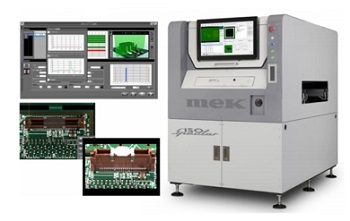
The ISO-Spector M1A is the new flagship full 3D AOI system from Mek (Marantz-Electronics). ISO-Spector M1A features the electronics industry’s highest hardware specifications and introduces an exceptionally convenient fast automatic programming method while achieving production ready inspection results with very short cycle times. See the system in action at SMT, Booth: 4-216.
The ISO-Spector M1A has a massive field of view (FoV) of 69 x 69mm (2.72” x 2.72”) and the industry’s largest 25 mega pixel camera with advanced lens optics. Multiple Moiré fringe projections enable high precision, shadow free measurement of heights up to 25 mm as well as 4 fully programmable side view high-res cameras able to actively inspect J- leads and other devices invisible to top side imagers.
The programming of the ISO-Spector M1A is exceptionally easy and programmer-independent. The artificial intelligence reduces the human element involved in the programming meaning that the inspection results are the same whether programmed by a beginner or by an expert. The AI learns the production process values of assembled and reflowed PCB’s and then recognizes defects based on hundreds of preset parameters. This is particularly significant in the inspection of solder joints, which are typically the most difficult and time consuming to program in AOI’s.
The large FoV combined with an industrial grade computer, ensure short cycle times even when fully utilized including foreign material detection across the complete printed circuit board area.
Offline programming is possible. The ISO-Spector integrates fully with Industry 4.0 specifications via the FIBER system for classification, repair, traceability and SPC.
About Mek (Marantz Electronics Ltd)
A former division of Marantz well known for its high quality Audio/Video products, Mek Japan (Marantz Electronics Kabushiki Kaisha), developed its first AOI system in 1994. Developed to inspect PCB assemblies for correct component placement and soldering, the company’s original AOI system was designed for use in Marantz factories. Proving to be a highly successful, cost-effective alternative to traditional human inspection, Mek developed its first generation commercial system in 1996. With a steadily growing installed base, MEK Japan and its European/American headquarters, Mek, have sold over 7000 units worldwide to date. Now well established as a leading force in AOI technologies, the company also manufactures a 5D post-print SPI system which combines 3D and 2D image processing methodologies to deliver unprecedented defect detection. At the beginning of March 2014 the company opened US offices in Las Vegas.
For more information, click here.


