


 Trouble in Your Tank: At 40 GHz, Everything Matters, Part 2
 It’s Only Common Sense: Stop Watching the Headlines and Start Watching the Opportunity
 The Right Approach: The Pros and Cons of PCB Vertical Integration


Researchers more than doubled the ability of a material to convert heat into electricity, which could help reduce the amount of wasted heat, and thus wasted fossil fuel, in daily activities and industries.
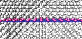
Image caption: Conceptual drawing of the superlattice in which spread electrons are confined to a narrow space to enhance thermoelectric conversion. (Image: Hokkaido University)
Researchers from Hokkaido University and their colleagues in Japan and Taiwan have improved the ability to transform wasted heat into usable electricity by significantly narrowing the space through which spread electrons move, according to a new study published in the journal Nature Communications("Double thermoelectric power factor of a 2D electron system").
More than 60% of energy produced by fossil fuels is lost as waste heat. One way to address this problem is to convert the wasted heat into electricity, known as thermoelectric energy conversion. However, improving the conversion rate has been difficult because of a trade-off relationship between the required properties within the material.
Thermoelectric materials convert heat into electricity when there is a temperature difference, a phenomenon known as the Seebeck effect. Scientists have been investigating ways to confine electrons to a narrow space as a way to enhance conversion rates. In 2007, researchers built an artificial superlattice composed of conducting ultrathin layers sandwiched by thick insulating layers. This method yielded higher voltage but did not improve conversion rates. Researchers have predicted that performance can be significantly improved if electrons with longer de Broglie wavelength, which means they are more spread, are confined into a narrow conducting layer, but it had not yet been proven experimentally.
The research team, led by Hiromichi Ohta of Hokkaido University, designed a superlattice in which electrons are spread by 30 percent wider as compared to previous experiments. This resulted in much higher voltage and doubled the thermoelectric conversion rate recorded from previous methods.
"This is a significant step forward towards reducing the amount of heat wasted by power plants, factories, automobiles, computers, and even human bodies" says Hiromichi Ohta of Hokkaido University.


