


 Knocking Down the Bone Pile: The Business Case for Component Reclamation
 Global Sourcing Spotlight: The Hidden Power of the Rep Network
 Smart Automation: When Traditional Depaneling Methods Reach Their Limits


Since the manufacture of X-ray inspection machines began at Nikon Metrology's Tring, UK factory in 1987, 1,000 Xi sources with an internal X-ray generator have been designed, produced and integrated into the company's XT V systems, in addition to numerous other sources for the XT H range of X-ray and computed tomography machines.
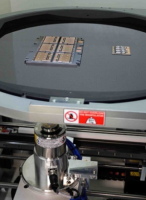
Image caption: The XT V 160 at IXYS UK Westcode contains the 1,000th Xi X-ray source to be manufactured at Nikon Metrology's factory in Tring, UK.
The latest Xi source has been incorporated into an XT V 160 electronics inspection system that is supporting quality assurance of power semiconductor device production at IXYS UK Westcode, Chippenham, UK. The X-ray inspection machine is being used to check whether the reflowed solder that attaches integrated circuits to contact pads on the direct copper bonded substrate boards is continuous, with a controlled level of voids.
The 160 kV Xi source is of integrated construction, unique to Nikon, which eliminates the need for a traditional, high voltage cable connecting the X-ray generator to the source. Maintenance costs are therefore lower, as such cables can be prone to failure and need regular maintenance.
As with all Nikon sources it is of open-tube design, giving low cost of ownership. As part of planned maintenance, replacement of the electron beam-producing filament can be scheduled during the year for a cost of a few pounds each time. Filament replacement takes minutes, so downtime is short.
By contrast, a sealed tube will last for a couple of years but can stop working without warning, perhaps at the worst possible time for the user. The manufacturer then has to be called in to renew the tube at a cost of many thousands of pounds and the machine is down for days.
Fiona Lambert, Process Engineer at IXYS UK Westcode commented, "I previously used a smaller Nikon 130 kV X-ray quality assurance system when I worked at an electronics company in South Wales, so I knew how easy their equipment is to use.
"After reviewing what else was on the market, it was clear that their 160 kV model would best suit our application. The Xi source allows high resolution to be maintained at high powers, which we need to penetrate a thick aluminium layer to evaluate solder quality.
"What I also like about the Nikon system is the easy access to the large stage, which allows me to place several, quite large components on it at the same time. The machine is fast in operation and the stage is easy to manipulate in multiple axes, so tilting, rotating and positioning as well as zooming the image on the screen is rapid.
"The software is also user-friendly and even works out automatically the percentage of voids in the solder, required to ensure the product meets rigorous specifications.”
A video of Fiona Lambert talking about the advantages of the Nikon Metrology XT V 160 can be watched below:


