


 The Chemical Connection Onshoring PCB Production—Daunting but Certainly Possible
 It’s Only Common Sense: The Phone Is Still Mightier Than the Keyboard


Ultimate Precision for Sensor Technology Using Qubits and Machine Learning
July 3, 2018 | Aalto UniversityEstimated reading time: 3 minutes
Extracting information quickly from quantum states is necessary for future quantum processors and super-sensitive detectors in existing technologies.
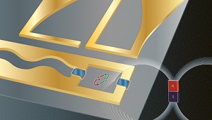
Image caption: An artificial atom realized from superconducting strips of aluminum on a silicon chip can be employed for the detection of magnetic fields. Image: Babi Brasileiro / Aalto University
There are limits to how accurately you can measure things. Think of an X-ray image: it is likely quite blurry and something only an expert physician can interpret properly. The contrast between different tissues is rather poor but could be improved by longer exposure times, higher intensity, or by taking several images and overlapping them. But there are considerable limitations: humans can safely be exposed to only so much radiation, and imaging takes time and resources.
A well-established rule of thumb is the so-called standard quantum limit: the precision of the measurement scales inversely with the square root of available resources. In other words, the more resources—time, radiation power, number of images, etc.—you throw in, the more accurate your measurement will be. This will, however, only get you so far: extreme precision also means using excessive resources.
A team of researchers from Aalto University, ETH Zurich, and MIPT and Landau Institute in Moscow have pushed the envelope and came up with a way to measure magnetic fields using a quantum system. They demonstrate a new method that combines quantum phenomena and machine learning to realise a magnetometer with accuracy beyond the standard quantum limit.
The detection of magnetic fields is important in a variety of fields, from geological prospecting to imaging brain activity. The researchers believe that their work is a first step towards of using quantum-enhanced methods for sensor technology.
“We wanted to design a highly efficient but minimally invasive measurement technique. Imagine, for example, extremely sensitive samples: we have to either use as low intensities as possible to observe the samples or push the measurement time to a minimum,” explains Sorin Paraoanu, leader of the Kvantti research group at Aalto University.
Their paper, published in the prestigious journal npj Quantum Information shows how to improve the accuracy of magnetic field measurements by exploiting the coherence of a superconducting artificial atom, a qubit. It is a tiny device made of overlapping strips of aluminium evaporated on a silicon chip—a technology similar to the one used to fabricate the processors of mobile phones and computers.
When the device is cooled to a very low temperature, magic happens: the electrical current flows in it without any resistance and starts to display quantum mechanical properties similar to those of real atoms. When irradiated with a microwave pulse—not unlike the ones in household microwave ovens—the state of the artificial atom changes. It turns out that this change depends on the external magnetic field applied: measure the atom and you will figure out the magnetic field.
But to surpass the standard quantum limit, yet another trick had to be performed using a technique similar to a widely-applied branch of machine learning, pattern recognition.
“We use an adaptive technique: first, we perform a measurement, and then, depending on the result, we let our pattern recognition algorithm decide how to change a control parameter in the next step in order to achieve the fastest estimation of the magnetic field,” explains Andrey Lebedev, corresponding author from ETH Zurich, now at MIPT in Moscow.
“This is a nice example of quantum technology at work: by combining a quantum phenomenon with a measurement technique based on supervised machine learning, we can enhance the sensitivity of magnetic field detectors to a realm that clearly breaks the standard quantum limit,” Lebedev says.
Share on:


Testimonial
"We’re proud to call I-Connect007 a trusted partner. Their innovative approach and industry insight made our podcast collaboration a success by connecting us with the right audience and delivering real results."
Julia McCaffrey - NCAB GroupSuggested Items
Smart Eye Collaborates with Sony on Next-Generation Interior Sensing and Iris Authentication
10/09/2025 | Smart EyeSmart Eye AB, the global leader in Interior Sensing AI and Driver Monitoring Systems (DMS), announced a collaboration with Sony Semiconductor Solutions Corporation (Sony) to integrate Smart Eye’s interior sensing and biometric authentication software with Sony’s newly released IMX775 RGB-IR image sensor.
SEMICON Europa 2025 to Highlight Innovations in Advanced Packaging, Fab Management, and MEMS and Imaging Sensors to Bolster Europe’s Semiconductor Resilience
10/03/2025 | SEMISemiconductor industry experts will convene at SEMICON Europa 2025, November 18-21 at Messe München in Munich, to explore the latest trends and innovations in advanced packaging and fab management.
MEMS & Imaging Sensors Summit to Spotlight Sensing Revolution for Europe’s Leadership
09/11/2025 | SEMIIndustry experts will gather November 19-20 at the SEMI MEMS & Imaging Sensors Summit 2025 to explore the latest breakthroughs in AI-driven MEMS and imaging optimization, AR/VR technologies, and advanced sensor solutions for critical defence applications.
Direct Imaging System Market Size to Hit $4.30B by 2032, Driven by Increasing Demand for High-Precision PCB Manufacturing
09/11/2025 | Globe NewswireAccording to the SNS Insider, “The Direct Imaging System Market size was valued at $2.21 Billion in 2024 and is projected to reach $4.30 Billion by 2032, growing at a CAGR of 8.68% during 2025-2032.”
I-Connect007’s Editor’s Choice: Five Must-Reads for the Week
07/04/2025 | Marcy LaRont, I-Connect007For our industry, we have seen several bullish market announcements over the past few weeks, including one this week by IDC on the massive growth in the global server market. We’re also closely watching global trade and nearshoring. One good example of successful nearshoring is Rehm Thermal Systems, which celebrates its 10th anniversary in Mexico and the official opening of its new building in Guadalajara.