


 The Government Circuit: New Council Now Helps Shape Policy Decisions in the Electronics Supply Chain
 Learning With Leo: Soldering—The Interpretation Problem
 Nolan’s Notes: The ROI of Setup Optimization


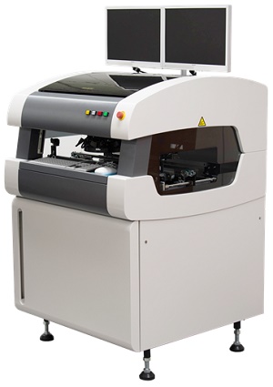
The new Mek PowerSpector BTL AOI systems offer synchronized inspection of the top and bottom side of PCBs after reflow, wave or selective soldering & placement of SMT & THT components.
Patented synchronized lighting technology delivers new capabilities. 9 cameras per side, with both heads inspecting the PCB at the same time, deliver fastest inspection times but without the high power lighting system of each head affecting the other inspection taking place. The elimination of flipping removes potential for stress on the assembly and improves long term reliability of solder joints.
The GTAz based bottom side inspection head has a clearance of 30mm from the PCB surface. An additional Z axis allows the head to be adjusted by 30mm to allow optimal flexibility for inspection inside solder frames and the correct adjustment of side cameras to further enhance defect identification capabilities. The 18.75u resolution of the main optics and the 13u resolution of the side cameras also give the option for 01005” (0402mm) SMD inspection including height verification of objects like pins and packages, as well as 3D chip height measurement.
The GDAz based top side inspection head combines a massive 60mm top clearance with full solder joint inspection via the 3D meniscus profiler. An additional 30mm Z-Axis, with autofocus option, allows the user to focus on the top of taller components. The side cameras with 20u resolution can be used to inspect side markings on components as well as verify accurate insertion using height verification.
Operator misjudgements of found defects are minimized by the true 3D Image defect display of 9-angle simultaneous microscopic views. Each defect is displayed with a magnification up to 50x (bottom up) or 30x (top down). This minimizes operator handling and reduces time spent on post-classification of defects using stationary microscopes
All images can be stored in the Mek’s Catch SQL database for review or post classification at any time after the actual inspection. For full tracking and tracing using your own MES system, the Catch system interfaces via its open SQL database or XML outputs.
The BTL is available in two different models; the PowerSpector 550BTL suitable for assemblies up to 5kg with a maximum dimension of up to 550x550mm (21.6”) and the PowerSpector 350BTL designed for medium Size PCB’s up to 350x250mm. (13.8"x9.8")
About Mek (Marantz Electronics Ltd)
A former division of Marantz well known for its high quality Audio/Video products, Mek Japan (Marantz Electronics Kabushiki Kaisha), developed its first AOI system in 1994. Developed to inspect PCB assemblies for correct component placement and soldering, the company’s original AOI system was designed for use in Marantz factories. Proving to be a highly successful, cost-effective alternative to traditional human inspection, Mek developed its first generation commercial system in 1996. With a steadily growing installed base, MEK Japan and its European/American headquarters, Mek, have sold over 7000 units worldwide to date. Now well established as a leading force in AOI technologies, the company also manufactures a 5D post-print SPI system which combines 3D and 2D image processing methodologies to deliver unprecedented defect detection. At the beginning of March 2014 the company opened US offices in Las Vegas. For more information, click here.


