


 The Chemical Connection Onshoring PCB Production—Daunting but Certainly Possible
 It’s Only Common Sense: The Phone Is Still Mightier Than the Keyboard


Brighter Microscopy Using Built-In Nanobulbs
July 16, 2018 | A*STAREstimated reading time: 2 minutes
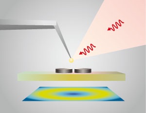
By using ultrafast laser pulses to join silicon and gold atoms into a new type of nanoparticle, researchers from A*STAR and ITMO University, Russia, have created a white-light source for applications including high-resolution characterization of biomolecules.
The wave nature of light imposes constraints on the resolution of conventional optical microscopes, no matter how intense the source. The process of diffraction spreads out light waves at the nanoscale and produces blurry images when objects are smaller than half the source beam’s wavelength.
Now, researchers have devised a way to beat the diffraction limit. Arseniy Kuznetsov and Yefeng Yu from the A*STAR Data Storage Institute have teamed up with colleagues at Russia’s ITMO University to improve near-field scanning optical microscopy (NSOM) devices. These microscopes embed optically active materials inside a sharp microscale tip. When positioned extremely close to a sample, the light-emitting tip generates evanescent waves capable of resolving items separated by just a few nanometers.
One drawback of NSOM is that implanted light sources, such as quantum dot crystals and photoactive molecules, tend to emit in narrow regions of the electromagnetic spectrum. This makes it difficult to use these materials for emerging ‘nanospectroscopy’ applications that detect a sample’s structural and optical features in ultra-fine detail; broad-spectrum white light that excites many components of a specimen simultaneously would be preferable.
Kuznetsov, Yu, and their colleagues realized that silicon nanoparticles, which exhibit wide-ranging luminescence after laser excitation, might solve this white light problem if they could be made more efficient at scales suitable for NSOM tips. To realize this goal, the team deposited a thin layer of silicon on top of a gold-coated substrate, and then exposed the material to bursts of ultra-fast lasers. Spherical silicon nanoparticles containing integrated gold regions were recovered from the ablation process.
“Normally, these two materials are unmixable — melting them together won’t produce a good alloy,” explains Kuznetsov. “But when the process happens with femtosecond laser pulses, we get a hybrid that solidifies in an unusual state.”
The researchers’ experiments revealed that the gold regions of the new material produced high-energy, ‘hot’ electrons that transferred to silicon crystals and helped them emit ultraviolet, visible, and infrared light. Attaching the hybrid particle to the end of a microscopic tip enabled them to scan nanoscale photonic devices and map out their optical response at high speeds.
“This mixture has unique photoluminescence properties that take advantage of both components,” says Kuznetsov. “We are working on ways to control their dimensions and nanocompositions.”
Share on:


Testimonial
"Advertising in PCB007 Magazine has been a great way to showcase our bare board testers to the right audience. The I-Connect007 team makes the process smooth and professional. We’re proud to be featured in such a trusted publication."
Klaus Koziol - atgSuggested Items
Beyond Design: The Fundamental Structure of Spectral Integrity
10/21/2025 | Barry Olney -- Column: Beyond DesignImpedance can be characterized in both the time and frequency domains. In the time domain, it influences how electromagnetic energy propagates through interconnects, affecting signal integrity and waveform fidelity. In the frequency domain, AC impedance determines how well the network can suppress noise and deliver clean power at a range of frequencies. AC impedance shapes how power rails respond to transient loads.
Light-curable Solutions for Reliable Electronics in Space Applications
10/15/2025 | Virginia Hogan, DymaxDesigning electronics for space environments, particularly those in low Earth orbit (LEO), requires careful consideration of materials that can withstand extreme conditions while supporting long-term reliability. Engineers designing satellite systems, aerospace instrumentation, and high-altitude platforms face a familiar set of challenges: contamination control, mechanical stress, thermal cycling, and manufacturability.
Is Glass Finally Coming of Age?
10/13/2025 | Nolan Johnson, I-Connect007Substrates, by definition, form the base of all electronic devices. Whether discussing silicon wafers for semiconductors, glass-and-epoxy materials in printed circuits, or the base of choice for interposers, all these materials function as substrates. While other substrates have come and gone, silicon and FR-4 have remained the de facto standards for the industry.
Global PCB Connections: Understanding Your Fabricator’s Capabilities (or Niche)
10/08/2025 | Markus Voeltz -- Column: Global PCB ConnectionsNot every PCB fabricator is a good fit for every design. This is something many seasoned OEMs and greenhorn designers learn the hard way. The industry is full of talented board shops: global giants, regional specialists, niche fabricators, and everything in between. But even the best shop can fail a job if it's not the right fit for that specific board, volume, or customer requirement.
American Standard Circuits to Exhibit at SMTA International
10/06/2025 | American Standard CircuitsAnaya Vardya, President, and CEO of American Standard Circuits/ASC Sunstone Circuits has announced that his company will once again exhibit at SMTA International 2025 to be held at the Donald E Stephens Convention Center in Rosemont, Illinois on October 19th through the 23rd, 2025.