


 The Chemical Connection: Onshoring PCB Production—Daunting but Certainly Possible
 It’s Only Common Sense: The Phone Is Still Mightier Than the Keyboard


UNSW Team Lands New Efficiency Breakthrough for Emerging Solar Cell Material
July 25, 2018 | UNSWEstimated reading time: 3 minutes
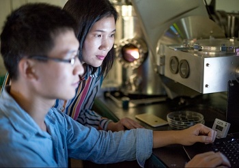
UNSW solar energy researcher and Scientia Fellow Dr Xiaojing Hao and her team have achieved two energy efficiency world records for the solar cell material of the future, sulfide kesterite.
Dr. Hao and her team broke the 10% efficiency barrier for not only sulfide kesterite but also for a standard sized kesterite solar cell, whether pure sulfide material or incorporating less-desirable selenium. The result, which is published in a paper in Nature Energy today, is the fourth consecutive efficiency record achieved by the group led by Dr. Hao in two years.
Dr. Hao says that while the energy efficiency is not yet at a level that can be used in industry, the results are promising for a material that is abundant and cheap to procure. "Sulfide kesterite is a compound made up of copper, zinc, tin and sulfur – four cheap and abundant elements in the Earth’s crust,” she says. “I call them green materials, because in addition to being abundant, they’re also non-toxic.”
Sulfide kesterite (Cu2ZnSnS4, also referred to as CZTS) is a thin-film semiconductor material derived from photovoltaic (PV) material CIGS (copper indium gallium (di)selenide) which is a commercialised high efficiency thin-film PV technology that has the added advantage of being able to be applied to flexible surfaces.
However, a drawback of CIGS is that indium is relatively rare and in high demand for use in flat panel displays (such as television screens, notebook screens, and touch screens), which means it is expensive. One of the challenges of solar cells is the reliance upon rare and toxic materials for use in thin-film solar cell production.
“The price of indium is already high and expected to keep going up, because the market for flat panel displays is growing,” Dr. Hao says.
Enter CZTS. By replacing indium and gallium with the plentiful zinc and tin, you have a compound that fulfils the criteria of being low cost, flexible, non-toxic and abundant.
“In addition to that, as a stand-alone thin-film PV, CZTS related material has a chance to be used in a tandem cell with silicon as its bandgap can be easily tuned over a wide range when alloying with other elements, making it well matched to the high bandgap requirements for the upper cells of tandem stacks,” Dr Hao explains.
“The key prerequisite for such development is we need to get the efficiency of CZTS to beyond 20 per cent for us to see total energy efficiency of more than 30 per cent,” Dr Hao says.
Another advantage to using sulfide kesterite is that manufacturing processes for CIGS are easily adaptable to producing CZTS. Adding the fact that the thin-film can be applied to flexible surfaces makes it an attractive alternative.
“The flexible PV cells are lightweight, extending their potential use for building integration and on other uneven surfaces such as cars or unmanned air vehicles (UAVs).”
So CZTS is cheap, abundantly sourced, flexible, non-toxic and easily integrated into existing manufacturing processes. Missing is the energy efficiency levels needed for the material to be used commercially.
Given the advances in efficiency made in the past few years – from 7.6% to 11% – Dr Hao believes she and her team are on the right track to achieving efficiency levels of 15 or 20 per cent. But she is under no illusion that it will happen overnight.
“For each efficiency change, we need a step-change technology to make it happen,” Dr. Hao says.
“With CZTS, there are still so many things that we don't know. Unravelling these unknowns is the most exciting adventure.”
She is quite excited about recent unpublished findings which could bring significant changes. To ensure these new findings are developed further, she will be applying for funding for a new project at the end of the year.
Dr. Hao says she is also investigating other ‘green materials’ similar to CZTS which are abundant, non-toxic and could be used in tandem with silicon, in a project with Professor Martin Green supported by an ARENA grant awarded last year.
Share on:


Testimonial
"Your magazines are a great platform for people to exchange knowledge. Thank you for the work that you do."
Simon Khesin - Schmoll MaschinenSuggested Items
Episode 6 of Ultra HDI Podcast Series Explores Copper-filled Microvias in Advanced PCB Design and Fabrication
10/15/2025 | I-Connect007I-Connect007 has released Episode 6 of its acclaimed On the Line with... American Standard Circuits: Ultra High Density Interconnect (UHDI) podcast series. In this episode, “Copper Filling of Vias,” host Nolan Johnson once again welcomes John Johnson, Director of Quality and Advanced Technology at American Standard Circuits, for a deep dive into the pros and cons of copper plating microvias—from both the fabricator’s and designer’s perspectives.
Nolan’s Notes: Tariffs, Technologies, and Optimization
10/01/2025 | Nolan Johnson -- Column: Nolan's NotesLast month, SMT007 Magazine spotlighted India, and boy, did we pick a good time to do so. Tariff and trade news involving India was breaking like a storm surge. The U.S. tariffs shifted India from one of the most favorable trade agreements to the least favorable. Electronics continue to be exempt for the time being, but lest you think that we’re free and clear because we manufacture electronics, steel and aluminum are specifically called out at the 50% tariff levels.
MacDermid Alpha & Graphic PLC Lead UK’s First Horizontal Electroless Copper Installation
09/30/2025 | MacDermid Alpha & Graphic PLCMacDermid Alpha Electronics Solutions, a leading supplier of integrated materials and chemistries to the electronics industry, is proud to support Graphic PLC, a Somacis company, with the installation of the first horizontal electroless copper metallization process in the UK.
Electrodeposited Copper Foils Market to Grow by $11.7 Billion Over 2025-2032
09/18/2025 | Globe NewswireThe global electrodeposited copper foils market is poised for dynamic growth, driven by the rising adoption in advanced electronics and renewable energy storage solutions.
MacDermid Alpha Showcases Advanced Interconnect Solutions at PCIM Asia 2025
09/18/2025 | MacDermid Alpha Electronics SolutionsMacDermid Alpha Electronic Solutions, a global leader in materials for power electronics and semiconductor assembly, will showcase its latest interconnect innovations in electronic interconnect materials at PCIM Asia 2025, held from September 24 to 26 at the Shanghai New International Expo Centre, Booth N5-E30