


 The Chemical Connection: Onshoring PCB Production—Daunting but Certainly Possible
 It’s Only Common Sense: The Phone Is Still Mightier Than the Keyboard


Flat Lenses Bring Tiny Features into Focus
August 8, 2018 | A*STAREstimated reading time: 2 minutes
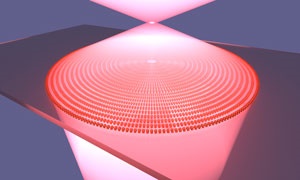
Simple flat lenses, incorporating nanoscale features, that outperform conventional bulk optics have been fabricated by scientists at A*STAR.
High-numerical-aperture optical lenses offer very high resolution and are particularly useful for low-light-intensity applications, such as single-photon optics. The numerical aperture is a measure of the conical angle of light that can be collected by the lens and, reciprocally, how tightly a beam of light can be focused. The larger the numerical aperture, the higher the resolution and the closer the lens can be to the object to be imaged. As the collection angle and, hence the amount of light collected from the object, approaches its theoretical maximum, the numerical aperture increases and gets closer to a value of one, the fundamental maximum for a lens in air.
However, high-numerical-aperture systems can be bulky, complex and expensive. And conventional glass-based optics rarely attain a numerical aperture above 0.95. Scientists from the A*STAR Data Storage Institute have now built a simple flat lens with a numerical aperture higher than 0.99.
“Previous attempts to make flat, high-numerical-aperture lenses ended up with devices that were very inefficient at its edges, where the light bends at very large angles,” explains A*STAR scientist Ramón Paniagua-Domínguez. “We proposed a new method to overcome this limitation using nanoantennas”
The ‘metalens’ created by Paniagua-Domínguez and his colleagues consists of arrays of silicon discs with various diameters on a substrate, each area designed to direct the light at a specific angle. All the areas were engineered to direct light into a specific point — the focus of the lens. The area responsible for giving the lens its high-numerical-aperture comprises pairs of nanometer-scale silicon cylinders, one larger than the other, which act like antennas for visible light. Using silicon rather than a metal reduces losses and makes the concept applicable across a wide range of wavelengths.
The dimensions of the nanoantennas — the disk diameter, disk separation and the pitch of the array — can be altered to suit the metalens’ wavelength range and specific application. For example, disk diameters of 190 and 150 nanometers redirect incoming red light at an angle of 82 degrees. This allowed the team to achieve a numerical aperture of 0.99 in their metalens, making it ideal for high-resolution applications.
“We are exploring more complex geometries to maximize the efficiency of the lens,” says Paniagua-Domínguez. “Plus, seeking other materials to expand the range of frequencies at which the lens works.”
Share on:


Testimonial
"Advertising in PCB007 Magazine has been a great way to showcase our bare board testers to the right audience. The I-Connect007 team makes the process smooth and professional. We’re proud to be featured in such a trusted publication."
Klaus Koziol - atgSuggested Items
PDN Optimization: Balancing Performance and Cost in SoC Designs
10/22/2025 | Zach Caprai. Siemens EDAThis article demonstrates advanced PDN optimization techniques through a real-world case study of AMD’s Versal adaptive SoC platform. Using the VCK190 evaluation kit featuring the Versal AI Core series VC1902 device, I’ll explore how effective PDN design and optimization can help meet demanding technical specifications while addressing essential business goals.
It’s Only Common Sense: Stop Whining About the Market—Outwork It
10/06/2025 | Dan Beaulieu -- Column: It's Only Common SenseWhenever the market hiccups or the industry cycle dips, I hear the same tired chorus: “The market is down. Customers aren’t buying. What can we do? We just have to wait it out.” Nonsense. If you think that by showing up, opening your doors, and waiting for the economy to smile kindly upon you, that success will follow, you are in the wrong business. Worse yet, you’re living in the wrong mindset. Most people don’t want to hear the truth that winners find business in down cycles. Losers blame the economy.
Empower Sets New Benchmark with 20x Faster Response and Breakthrough Sustainability Demonstrated at OCP Global Summit 2025
09/25/2025 | Empower SemiconductorEmpower Semiconductor, the world leader in powering AI-class processors, announced that its Crescendo chipset, an artificial intelligence (AI) and high-performance computing (HPC) processor true vertical power delivery platform, is available now for final sampling, with mass production slated for late 2025.
Transforming the Industry: Advint's Mission in Metallization
09/18/2025 | Marcy LaRont, PCB007 MagazineWith three decades of experience in engineering, research, and operations in blue-chip organizations, including Boeing and Honeywell, Venkat Raja has developed a passion for electroplating. In 2018, he founded Advint Incorporated, an electroplating advisory and training services firm dedicated to solving operational challenges, enhancing efficiency, and providing specialized training programs.
Alternative Manufacturing, Inc. (AMI) Announces Commitment to Excellence in Industrial, Defense, Aerospace, Renewables, and Robotics Markets
09/16/2025 | Alternative Manufacturing, Inc.Alternative Manufacturing, Inc. (AMI), a 100% employee-owned contract manufacturer, proudly reaffirms its leadership in the electronics manufacturing services (EMS) industry with a continued commitment to delivering high-quality PCBAs and box builds across the industrial, defense, aerospace, renewable energy, and robotics markets.