


 The Chemical Connection: Onshoring PCB Production—Daunting but Certainly Possible
 It’s Only Common Sense: The Phone Is Still Mightier Than the Keyboard


Introducing the Latest in Textiles: Soft Hardware
August 9, 2018 | MITEstimated reading time: 4 minutes
The latest development in textiles and fibers is a kind of soft hardware that you can wear: cloth that has electronic devices built right into it.
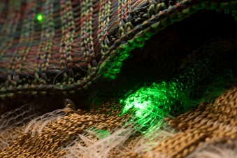
Image Caption: For the first time, the researchers from MIT and AFFOA have produced fibers with embedded electronics that are so flexible they can be woven into soft fabrics and made into wearable clothing.
Researchers at MIT have now embedded high speed optoelectronic semiconductor devices, including light-emitting diodes (LEDs) and diode photodetectors, within fibers that were then woven at Inman Mills, in South Carolina, into soft, washable fabrics and made into communication systems. This marks the achievement of a long-sought goal of creating “smart” fabrics by incorporating semiconductor devices — the key ingredient of modern electronics — which until now was the missing piece for making fabrics with sophisticated functionality.
This discovery, the researchers say, could unleash a new “Moore’s Law” for fibers — in other words, a rapid progression in which the capabilities of fibers would grow rapidly and exponentially over time, just as the capabilities of microchips have grown over decades.
A spool of fine, soft fiber made using the new process shows the embedded LEDs turning on and off to demonstrate their functionality. The team has used similar fibers to transmit music to detector fibers, which work even when underwater. (Courtesy of the researchers)
Optical fibers have been traditionally produced by making a cylindrical object called a “preform,” which is essentially a scaled-up model of the fiber, then heating it. Softened material is then drawn or pulled downward under tension and the resulting fiber is collected on a spool.
The key breakthrough for producing these new fibers was to add to the preform light-emitting semiconductor diodes the size of a grain of sand, and a pair of copper wires a fraction of a hair’s width. When heated in a furnace during the fiber-drawing process, the polymer preform partially liquified, forming a long fiber with the diodes lined up along its center and connected by the copper wires.
In this case, the solid components were two types of electrical diodes made using standard microchip technology: light-emitting diodes (LEDs) and photosensing diodes. “Both the devices and the wires maintain their dimensions while everything shrinks around them” in the drawing process, Rein says. The resulting fibers were then woven into fabrics, which were laundered 10 times to demonstrate their practicality as possible material for clothing.
“This approach adds a new insight into the process of making fibers,” says Rein, who was the paper’s lead author and developed the concept that led to the new process. “Instead of drawing the material all together in a liquid state, we mixed in devices in particulate form, together with thin metal wires.”
One of the advantages of incorporating function into the fiber material itself is that the resulting fiber is inherently waterproof. To demonstrate this, the team placed some of the photodetecting fibers inside a fish tank. A lamp outside the aquarium transmitted music (appropriately, Handel’s “Water Music”) through the water to the fibers in the form of rapid optical signals. The fibers in the tank converted the light pulses — so rapid that the light appears steady to the naked eye — to electrical signals, which were then converted into music. The fibers survived in the water for weeks.
Though the principle sounds simple, making it work consistently, and making sure that the fibers could be manufactured reliably and in quantity, has been a long and difficult process. Staff at the Advanced Functional Fabric of America Institute, led by Jason Cox and Chia-Chun Chung, developed the pathways to increasing yield, throughput, and overall reliability, making these fibers ready for transitioning to industry. At the same time, Marty Ellis from Inman Mills developed techniques for weaving these fibers into fabrics using a conventional industrial manufacturing-scale loom.
“This paper describes a scalable path for incorporating semiconductor devices into fibers. We are anticipating the emergence of a ‘Moore’s law’ analog in fibers in the years ahead,” Fink says. “It is already allowing us to expand the fundamental capabilities of fabrics to encompass communications, lighting, physiological monitoring, and more. In the years ahead fabrics will deliver value-added services and will no longer just be selected for aesthetics and comfort.”
He says that the first commercial products incorporating this technology will be reaching the marketplace as early as next year — an extraordinarily short progression from laboratory research to commercialization. Such rapid lab-to-market development was a key part of the reason for creating an academic-industry-government collaborative such as AFFOA in the first place, he says. These initial applications will be specialized products involving communications and safety. “It's going to be the first fabric communication system. We are right now in the process of transitioning the technology to domestic manufacturers and industry at an unprecendented speed and scale,” he says.
In addition to commercial applications, Fink says the U.S. Department of Defense — one of AFFOA’s major supporters — “is exploring applications of these ideas to our women and men in uniform.”
Beyond communications, the fibers could potentially have significant applications in the biomedical field, the researchers say. For example, devices using such fibers might be used to make a wristband that could measure pulse or blood oxygen levels, or be woven into a bandage to continuously monitor the healing process.
The research was supported in part by the MIT Materials Research Science and Engineering Center (MRSEC) through the MRSEC Program of the National Science Foundation, by the U.S. Army Research Laboratory and the U.S. Army Research Office through the Institute for Soldier Nanotechnologies. This work was also supported by the Assistant Secretary of Defense for Research and Engineering.
Share on:


Testimonial
"Advertising in PCB007 Magazine has been a great way to showcase our bare board testers to the right audience. The I-Connect007 team makes the process smooth and professional. We’re proud to be featured in such a trusted publication."
Klaus Koziol - atgSuggested Items
Episode 6 of Ultra HDI Podcast Series Explores Copper-filled Microvias in Advanced PCB Design and Fabrication
10/15/2025 | I-Connect007I-Connect007 has released Episode 6 of its acclaimed On the Line with... American Standard Circuits: Ultra High Density Interconnect (UHDI) podcast series. In this episode, “Copper Filling of Vias,” host Nolan Johnson once again welcomes John Johnson, Director of Quality and Advanced Technology at American Standard Circuits, for a deep dive into the pros and cons of copper plating microvias—from both the fabricator’s and designer’s perspectives.
Nolan’s Notes: Tariffs, Technologies, and Optimization
10/01/2025 | Nolan Johnson -- Column: Nolan's NotesLast month, SMT007 Magazine spotlighted India, and boy, did we pick a good time to do so. Tariff and trade news involving India was breaking like a storm surge. The U.S. tariffs shifted India from one of the most favorable trade agreements to the least favorable. Electronics continue to be exempt for the time being, but lest you think that we’re free and clear because we manufacture electronics, steel and aluminum are specifically called out at the 50% tariff levels.
MacDermid Alpha & Graphic PLC Lead UK’s First Horizontal Electroless Copper Installation
09/30/2025 | MacDermid Alpha & Graphic PLCMacDermid Alpha Electronics Solutions, a leading supplier of integrated materials and chemistries to the electronics industry, is proud to support Graphic PLC, a Somacis company, with the installation of the first horizontal electroless copper metallization process in the UK.
Electrodeposited Copper Foils Market to Grow by $11.7 Billion Over 2025-2032
09/18/2025 | Globe NewswireThe global electrodeposited copper foils market is poised for dynamic growth, driven by the rising adoption in advanced electronics and renewable energy storage solutions.
MacDermid Alpha Showcases Advanced Interconnect Solutions at PCIM Asia 2025
09/18/2025 | MacDermid Alpha Electronics SolutionsMacDermid Alpha Electronic Solutions, a global leader in materials for power electronics and semiconductor assembly, will showcase its latest interconnect innovations in electronic interconnect materials at PCIM Asia 2025, held from September 24 to 26 at the Shanghai New International Expo Centre, Booth N5-E30