


 Driving Innovation: Mechanical and Optical Processes During Rigid-flex Production
 It’s Only Common Sense: Your Biggest Competitor Is Complacency
 The Chemical Connection: Onshoring PCB Production—Daunting but Certainly Possible


Taking a Closer Look at Unevenly Charged Biomolecules
August 22, 2018 | AIP.orgEstimated reading time: 1 minute
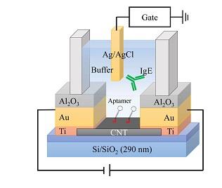
In clinical diagnostics, it is critical to monitor biomolecules in a simple, rapid and sensitive way. Clinicians most often monitor antibodies because these small proteins attach to antigens, or foreign substances, we face every day. Most biomolecules, however, have complicated charge characteristics, and the sensor response from conventional carbon nanotube systems can be erratic. A team in Japan recently revealed how these systems work and proposed changes to dramatically improve biomolecule detection.
These researchers demonstrated a new technique to detect, measure and analyze biomolecules with inhomogeneous charge distributions by adjusting the solution in which they monitor the biomolecule. They used carbon nanotube thin film transistors (CNT-TFTs) to zero in on the precise amount of a specific biomolecule is in a specimen.
CNT-TFT biosensors use immune antibody receptors called aptamers to detect the net electric charge of the part of the target molecule. After scientists identify a molecule, an antibody is made to attach to it in solution. That antibody then connects to an aptamer on a thin film of carbon nanotubes that converts the connection into an electrical signal for sensor detection. With this enhanced sensor response, researchers can determine the Debye length, or the distance between a point charge and the molecule, to map out a molecule’s uneven charge distributions.
The group discovered that they had to look at how the charges were distributed close to a molecule’s surface to understand the complicated behavior in the sensor signal. “Despite being the same target molecule, the polarities of the sensor response are completely different from positive or negative,” said Ryota Negishi, an author on the paper.
“We achieved the improvement of dynamic range by using low concentration of buffer solution,” Negishi said. “As a result, we clarified the mechanism of complicated sensor response which has not been clarified in previous reports.”
Many different features of an experiment can affect a molecule’s Debye length, so these results show promise for further controlling sensors and modifying their dynamic range.
Next, Negishi and his colleagues hope to find a way to use their findings in more real-life scenarios. “For practical application, it is essential to develop a sensing technology that can be detected under high concentration conditions close to blood.”
Share on:


Testimonial
"Our marketing partnership with I-Connect007 is already delivering. Just a day after our press release went live, we received a direct inquiry about our updated products!"
Rachael Temple - AlltematedSuggested Items
Sealed for Survival: Potting Electronics for the Toughest Environments
10/29/2025 | Beth Massey, MacDermid Alpha Electronics SolutionsElectronics deployed in harsh conditions face relentless threats from vibration, impact, chemical contaminants, airborne pollutants, and moisture, conditions that can quickly lead to failure without robust protection. Potting, the process of encapsulating electronics in a protective polymer, is a widely used strategy to safeguard devices from both environmental and mechanical hazards.
Sensors: The Invisible Force Behind Modern Convenience and Safety
10/24/2025 | Sanjeev Mane, Brooks AutomationSensors and sensor technology are fundamental components of modern life that drive innovation across various electronics and devices. From smartphones to industrial machinery, these small but powerful tools enable seamless interaction with the environment, ensuring efficiency and safety. This article serves as an introduction and overview of sensor technology, highlighting its significance in modern applications and its growing importance in the market as we embrace smarter, more connected systems.
ZenaTech Advances Taiwan Facility to Commissioning for NDAA-Compliant Drone Component Production
10/08/2025 | Globe NewswireZenaTech, Inc., a business technology solution provider specializing in AI (Artificial Intelligence) drones, Drone as a Service (DaaS), Enterprise SaaS, and Quantum Computing solutions, announces that its Taipei, Taiwan-based Spider Vision Sensors (SVS) subsidiary has advanced to the commissioning phase and assembly line setup at its recently leased 16,000 square-foot drone components manufacturing facility.
Interlink Electronics Awarded FDA SBIR Grant to Advance Electrochemical Sensors for Food Safety and Quality Monitoring
10/03/2025 | Globe NewswireInterlink Electronics, Inc., a global leader in sensor technology and printed electronic solutions, today announced that its Gas and Environmental Solutions division has received a $200,000 SBIR Phase 1 grant from the Food and Drug Administration (FDA).
Tobii, STMicroelectronics Enter Mass Production of Breakthrough Interior Sensing Technology
10/02/2025 | Globe NewswireTobii, the global leader in eye tracking and pioneer of attention computing, and STMicroelectronics, a global semiconductor leader serving customers across the spectrum of electronics applications, announced the beginning of mass production of an advanced interior sensing system for a premium European carmaker.