


 The Marketing Minute: If Your Marketing Budget Gets Cut in Half, Then What?
 Punching Out: How Are the Big Boys in Electronics Doing?
 It’s Only Common Sense: Complexity Is the Enemy of Profit


Atotech to Present and Exhibit at the 38th IEMT Conference
August 29, 2018 | AtotechEstimated reading time: 2 minutes
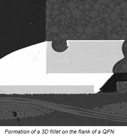
Atotech will participate in the 38th International Electronics Manufacturing Technology (IEMT) Conference 2018. Atotech will exhibit in Booth 20 and present the paper “Improving Reliability by Forming a 3D Connection for Quad Flat No-lead ICs using Immersion Tin.” The conference will be held at the Ramada Plaza in Melaka, Malaysia, from September 4 to 6, 2018.
As a keynote presenter, Rick Nichols, Global Product Manager Surface Finishing at Atotech Group, will speak in session D6 on September 6, from 10:30 am to 12:10 pm. “The surfaces of Quad Flat No-lead (QFN) devices are usually electrolytically tin plated on the contacts and heat sink. This technique limits the connection to the bottom surface of the IC and is only two dimensional,” Nichols said. “The incorporation of an immersion tin process will make a 3D connection or fillet possible.”
In his presentation, Nichols will explore the processes required and highlight the main benefits, which are quality enhancement and the potential to improve the reliability of automatic optical inspection (AOI).
Traditionally, the IEMT Conference 2018 focuses on new and future technology trends and intelligent innovations. So, what can one expect from Atotech this year? Atotech announced a special product feature on next generation copper pillar plating and an inventive non-etching adhesion promoter for advanced packaging substrates.
Spherolyte Cu RDL/ Pillar 3
Spherolyte Cu RDL/Pillar 3 is the next generation of high speed copper pillar plating for advanced packaging, permitting high speed pillar plating of up to 4.0 µm per minute. Its primary feature is a pure copper deposition, which is achieved through a lower incorporation of organic impurities of the additive system. This leads to lower void formation at the intermetallic phase and allows the elimination of the nickel plating step. Spherolyte Cu RDL/Pillar 3 also enables flat and recess free pillar plating, even when plating on top of μ-vias.
NovaBond IT
NovaBond IT is a new and innovative non-etching adhesion promoter (NEAP) for inner-layer bonding and soldermask pretreatment. It combines the benefits of a non-etching surface treatment with enhanced peel strength and thermal reliability. This superior performance is achieved on standard ABF build-up films as well as soldermasks and high frequency materials. NovaBond IT promotes the formation of a nano-dimensional copper oxide structure, adding a superb surface area increase to the conductors, but hardly contributing to the surface roughness.
Visitors to the show are invited to stop by and meet the Atotech team at booth number 20 to find out more about the special featured products or simply to discuss future industry and technology trends and innovations with Atotech’s leading experts and specialists on site.
About Atotech
Atotech is one of the world’s leading manufacturers of specialty chemicals and equipment for the printed circuit board, IC-substrate and semiconductor industries, as well as for the decorative and functional surface finishing industries. Atotech has annual sales of USD1.2 billion (2017). The company is fully committed to sustainability – we develop technologies to minimize waste and to reduce environmental impact. Atotech has its headquarters in Berlin, Germany, and employs about 4,000 people in over 40 countries.
Share on:


Testimonial
"We’re proud to call I-Connect007 a trusted partner. Their innovative approach and industry insight made our podcast collaboration a success by connecting us with the right audience and delivering real results."
Julia McCaffrey - NCAB GroupSuggested Items
I-Connect007 Releases The Printed Circuit Designer’s Guide to… Direct Metallization: A Guide to Complex PCB Fabrication
05/15/2026 | I-Connect007As PCB complexity continues to accelerate, fabricators and OEMs are reevaluating long-standing manufacturing processes to meet the demands of AI, HDI, advanced packaging, and next-generation electronics. To address these evolving challenges, I-Connect007 is proud to announce the release of The Printed Circuit Designer’s Guide to… Direct Metallization: A Guide to Complex PCB Fabrication, authored by MacDermid Alpha Solution’s Carmichael Gugliotti.
Driving Innovation: Selecting the Right Laser Source
04/28/2026 | Simon Khesin -- Column: Driving InnovationWhen I first joined Schmoll Maschinen, I brought experience from almost every PCB process, except for laser. As I immersed myself in laser processing, I realized why it can seem so daunting to a newcomer. The complexity arises from three intersecting factors: A vast variety of laser sources: CO2, UV-nano, green-pico, UV-pico, IR-pico, and others; a diverse range of applications: Drilling, cutting, ablation, and more; and an extensive list of materials: These have vastly different absorption rates. Choosing the right machine or laser source is rarely trivial. Even for experienced engineers, answering "Which source is best?" requires examining the business's specific goals.
Institute of Circuit Technology Spring Seminar 2026: A Bright Future in Europe
04/23/2026 | Pete Starkey, I-Connect007Through the leafy lanes and spring flowers of Warwickshire and back to Meridan, the traditional centre of England, and now officially part of the Metropolitan Borough of Solihull in the county of the West Midlands, I attended the Annual General Meeting and Spring Seminar of the Institute of Circuit Technology (ICT) on April 14. Out of the AGM came notable changes in leadership at the top of the Institute: the retirement of Mat Beadel as chair and Emma Hudson as technical director. Effective May 1, Steve Driver is the new chair, and Alun Morgan is the new technical director.
ACCM Unveils Negative and Near-zero CTE Materials for Large-Format AI Chips
04/21/2026 | Advanced Chip and Circuit MaterialsAdvanced Chip and Circuit Materials, Inc. (ACCM) has launched two new materials: Celeritas HM50, with a negative coefficient of thermal expansion (CTE) of -8 ppm/°C to offset the positive CTE and expansion of copper with temperature on circuit boards, and Celeritas HM001, with near-zero CTE and the low-loss performance needed for high-speed signal layers to 224 Gb/s and faster in artificial intelligence (AI) circuits.
Fresh PCB Concepts: Designing PCBs for Harsh Environments—Reliability Is Engineered Upstream
04/23/2026 | Team NCAB -- Column: Fresh PCB ConceptsWhen engineers hear the phrase “harsh environment,” they usually think of the extreme temperature swings, vibration and shock, pressure changes, or radiation in aerospace. However, aerospace is not the only harsh environment where electronic assemblies must survive. Automotive power electronics, downhole oil and gas tools, marine controls, rail systems, defense platforms, and industrial automation equipment all expose PCBs to environments that are equally unforgiving. The stress mechanisms may differ, but the physics does not.