


 Driving Innovation: Mechanical and Optical Processes During Rigid-flex Production
 It’s Only Common Sense: Your Biggest Competitor Is Complacency
 The Chemical Connection: Onshoring PCB Production—Daunting but Certainly Possible


First Truly Black Solar Modules Roll off Industrial Production Line
September 11, 2018 | Aalto UniversityEstimated reading time: 2 minutes
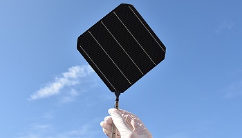
A 2011 invention made by Aalto University’s researchers has proceeded from concept to reality. Just a few years ago, the researchers obtained the record efficiency of 22% in the lab for nanostructured solar cells using atomic layer deposition. Now with the help of industrial partners and joint European collaboration, the first prototype modules have been manufactured on an industrial production line.
'Our timing could not have been better,' Professor Hele Savin, who led the research, was pleased to share. Indeed, 2018 is commonly called the 'Year of Black Silicon' due to its rapid expansion in the photovoltaic (PV) industry. It has enabled the use of diamond-wire sawing in multicrystalline silicon, which reduces costs and environmental impact. However, there is still plenty of room for improvement as the current black silicon used in industry consists of shallow nanostructures that lead to sub-optimal optical properties and require a separate antireflection coating.
Aalto’s approach consists of using deep needle-like nanostructures to make an optically perfect surface that eliminates the need for the antireflection coatings. Their industrial production, however, was not an easy task. 'We were worried that such a fragile structure would not survive the multi-step mass production, because of rough handling by robots or module lamination.'
Luckily, the concerns were proven not to be an issue. The cells and modules were truly black when they came out from production and had no signs of damage. The best module was producing energy with more than 20% efficiency. In addition to excellent optical properties, the researchers were positively surprised that their black cells had additional unexpected benefits, such as a high tolerance towards impurities and much better long-term stability as compared to the industry standard reference cells.
How expensive is black silicon technology? 'Questions related to techno-economical analysis are always difficult, especially for material scientists like us. Luckily, we got help from people with related expertise,“ Savin answers. The project partners provided data to Profesor Joshua Pearce at Michigan Tech University, whose preliminary calculations indicate that, while deep nanostructures are expensive to fabricate, the higher performance of the end product could balance out the total costs, e.g. due to a lower amount of process steps.
The R&D project (BLACK) was part of the Solar-ERANET network and was funded by the EU and Business Finland. The project partners included Spain’s Universitat Politècnica de Catalunya, Germany’s Solar World Innovations GmbH and Finnish-based companies Beneq, Naps Solar Systems, Cencorp, Okmetic, and Fortum. The project key findings will be presented by PhD student Toni Pasanen at the European Photovoltaic Solar Energy Conference in Brussels at the end of September 2018, where he will also receive an award in 'recognition of the most remarkable and outstanding research work in the field of PV'.
Share on:


Testimonial
"Advertising in PCB007 Magazine has been a great way to showcase our bare board testers to the right audience. The I-Connect007 team makes the process smooth and professional. We’re proud to be featured in such a trusted publication."
Klaus Koziol - atgSuggested Items
I-Connect007 Welcomes New Columnist: Leo Lambert, EPTAC
10/30/2025 | I-Connect007I-Connect007 is excited to announce a column by Leo Lambert, an industry veteran with 40 years of experience, an award winner, and technical director at EPTAC. This column, Learning With Leo, will explore the evolution and related challenges of electronics product assembly, especially as it relates to training.
Better Sustainability Policies for Electronics
10/29/2025 | Diana Radovan, Global Electronics AssociationI joined the Global Electronics Association in August 2025 as the director of sustainability policy. Since then, much has happened in terms of geopolitics and in the development and re-envisioning of sustainability policies in the industry. While the European Commission has released several legislative packages to simplify sustainability requirements (“omnibus”), these developments haven’t yet settled and are not in effect. Given the many recent and ongoing public consultations, with often conflicting input from a broad range of stakeholders, final negotiations remain rather polarized among policymakers.
SMTAI 2025 Review: Reflecting on a Pragmatic and Forward-looking Industry
10/27/2025 | Marcy LaRont, I-Connect007Leaving the show floor on the final afternoon of SMTA International last week in Rosemont, Illinois, it was clear that the show remains a grounded, technically driven event that delivers a solid program, good networking, and an easy space to commune with industry colleagues and meet with customers.
Come Together: Tom Marktscheffel Used Data to Build CFX and a Global Factory Standard
10/27/2025 | Sandy Gentry, Community MagazineWhen Tom Marktscheffel, director of product management software solutions at ASMPT, looks back on his nearly three decades in electronics manufacturing, one word stands out: data. “Data is the new gold,” he says. Without it, automation, artificial intelligence, and the factory of the future are impossible. With it, the industry can move from manual, error-prone processes to smart, connected systems that make real-time decisions.
Simplifying Software Integration for Every Factory
10/22/2025 | Nolan Johnson, SMT007 MagazineAs a leading provider of factory digitalization solutions for electronics manufacturers, Cogiscan is at the heart of the software integration process. Davina McDonnell, director of marketing and product management, discusses how Cogiscan ensures that customers are ready to integrate and what it looks for to ensure a quick and appropriate installation.