


 Driving Innovation: Mechanical and Optical Processes During Rigid-flex Production
 It’s Only Common Sense: Your Biggest Competitor Is Complacency
 The Chemical Connection: Onshoring PCB Production—Daunting but Certainly Possible


Introducing the ‘Smart Mirror’
September 19, 2018 | NISTEstimated reading time: 4 minutes
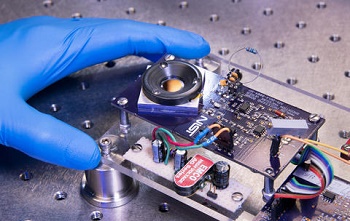
Lasers play roles in many manufacturing processes, from welding car parts to crafting engine components with 3D printers.* To control these tasks, manufacturers must ensure that their lasers fire at the correct power.
But to date, there has been no way to precisely measure laser power during the manufacturing process in real time, while lasers are cutting or melting objects, for example. Without this information, some manufacturers may have to spend more time and money assessing whether their parts meet manufacturing specifications after production.
To address this need, researchers from the National Institute of Standards and Technology (NIST) have been developing a laser power sensor that could be built into manufacturing devices for real-time measurements. They present the results from their latest prototype in an October 2018 issue of IEEE Sensors.
The new device works in a similar way to a previous sensor made by the team, which uses radiation pressure, or the force that light exerts on an object. But unlike their older device—a shoebox-sized “Radiation Pressure Power Meter (RPPM) for ultrahigh-power lasers of thousands of watts—the chip-sized “smart mirror” is designed for lasers of hundreds of watts, the range typically used for manufacturing processes.
“It’s still a radiation-pressure power meter, but it’s much smaller and much faster,” with 250 times the measurement speed of their larger sensor, said NIST’s John Lehman. The smart mirror is also about 40 times more sensitive than the RPPM.
The kinds of manufacturing processes that could potentially use this new technology include everything from airplanes and automobiles to cellphones and medical devices. The smart mirror could also be integrated into machines employed in additive manufacturing, a type of 3D printing that builds an object layer by layer, often using a laser to melt the materials that form the object.
Someday, the researchers say, these tiny meters could be in every additive manufacturing machine and in every laser weld head.
“This would put the high accuracy of NIST power measurements directly in the hands of operators, providing standardized quality assurance across laser-based systems and helping to accelerate the process of part qualification,” which ensures that manufactured objects meet engineering specifications, said NIST’s Alexandra B. Artusio-Glimpse.
New vs. Old
Conventional techniques for gauging laser power require an apparatus that absorbs all the energy from the beam as heat. Measuring the temperature change allows researchers to calculate the laser’s power.
The trouble with this traditional method is that if the measurement requires absorbing all the energy from the laser beam, then manufacturers can’t measure the beam while it’s actually being used for something.
Radiation pressure solves this problem. Light has no mass, but it does have momentum, which allows it to produce a force when it strikes an object. A 1-kilowatt (kW) laser beam has a small but noticeable force—about the weight of a grain of sand.
By shining a laser beam on a reflective surface, and then measuring how much the surface moves in response to light’s pressure, researchers can both measure the laser’s force (and, therefore, its power) and also use the light that bounces off the surface directly for manufacturing work.
How It Works
The NIST team’s previous RPPM, for multi-kW beams, works by shining the laser onto essentially a laboratory weighing scale, which depresses as the light hits it. But that device is too big to be integrated into welding heads or 3D printers. Researchers also wanted a system that would be more sensitive to the significantly smaller forces used for everyday manufacturing processes.
Instead of employing a laboratory balance, the new “smart mirror” works essentially as a capacitor, a device that stores electric charge. The sensor measures changes in capacitance between two charged plates, each about the size of a half dollar.
The top plate is coated with a highly reflective mirror called a distributed Bragg reflector, which uses alternating layers of silicon and silicon dioxide. Laser light hitting the top plate imparts a force that causes that plate to move closer to the bottom plate, which changes the capacitance, its ability to store electric charge. The higher the laser power, the greater the force on the top plate.
Laser light in the range used for manufacturing—in the hundreds of watts range—is not powerful enough to move the plate very far. That means that any physical vibrations in the room could cause that top plate to move in a way that wipes out the tiny signal it’s designed to measure.
So NIST researchers made their sensor insensitive to vibration. Both the top and bottom plates are attached to the device by springs. Ambient influences, such as vibrations if someone closes a door in the room or walks past the table, cause both plates to move in tandem. But a force that affects only the top plate causes it to move independently.
“If the device gets physically moved or vibrated, both plates move together,” Lehman said. “So the net force is strictly the radiation pressure, rather than any ambient influences.”
With this technique in place, the sensor can make precise, real-time power measurements for lasers of hundreds of watts, with a background noise level of just 2.5 watts.
“I’m just surprised how well it works. I’m really excited about it,” Lehman said. “If you told me two years ago that we’d do this, I’d say ‘no way!’”
Right now, the prototype sensor has been tested at a laser power of 250 watts. With further work, that range will likely extend to about 1 kW on the high end and below 1 watt on the low end. Lehman and colleagues are also working to improve the sensitivity and stability of the device.
Share on:


Testimonial
"Our marketing partnership with I-Connect007 is already delivering. Just a day after our press release went live, we received a direct inquiry about our updated products!"
Rachael Temple - AlltematedSuggested Items
Henger Microelectronics Expands Global Footprint with Major Equipment Shipment to Southeast Asia
10/31/2025 |Henger Microelectronics has reached a major milestone in its global expansion strategy with the successful shipment of advanced plasma etching and cleaning systems, along with automation equipment, to multiple countries and regions across Southeast Asia. This achievement marks a significant step forward in the company’s international growth and reinforces its position as a leading force in the global plasma equipment industry.
PCBAA Names Industry Veteran Dan Weber to Board of Directors
10/31/2025 | PCBAAThe Printed Circuit Board Association of America has added Dan Weber, Executive Vice President and General Counsel at TTM Technologies, to the PCBAA board of directors.
KLA Reports Fiscal Q1 2026 Results
10/31/2025 | PRNewswireKLA Corporation announced financial and operating results for its first quarter of fiscal year 2026, which ended on Sept. 30, 2025, and reported GAAP net income of $1.12 billion and GAAP net income per diluted share of $8.47 on revenues of $3.21 billion.
Samsung Teams With NVIDIA to Lead the Transformation of Global Intelligent Manufacturing Through New AI Megafactory
10/31/2025 | SamsungSamsung Electronics today announced plans to create a new AI Megafactory in collaboration with NVIDIA, marking a major milestone in the company’s efforts to lead the global paradigm shift toward AI-driven manufacturing.
Fresh PCB Concepts: Resilience and Renewal in Domestic PCB Manufacturing
10/30/2025 | Team NCAB -- Column: Fresh PCB ConceptsAs veterans of PCB manufacturing, we have spent much of our careers walking factory floors, examining copper circuits under microscopes, and troubleshooting plating lines when they go awry at 2 a.m. We can say with confidence that PCBs are the unsung heroes of modern life. They’re in everything, from toothbrushes and thermostats to satellites and defense systems.