


 It’s Only Common Sense: The Phone Is Still Mightier Than the Keyboard
 The Marketing Minute: Marketing With Layers


New NIST Method Measures 3D Polymer Processing Precisely
October 9, 2018 | NISTEstimated reading time: 2 minutes
Recipes for three-dimensional (3D) printing, or additive manufacturing, of parts have required as much guesswork as science. Until now.
Resins and other materials that react under light to form polymers, or long chains of molecules, are attractive for 3D printing of parts ranging from architectural models to functioning human organs. But it’s been a mystery what happens to the materials’ mechanical and flow properties during the curing process at the scale of a single voxel. A voxel is a 3D unit of volume, the equivalent of a pixel in a photo.
Now, researchers at the National Institute of Standards and Technology (NIST) have demonstrated a novel light-based atomic force microscopy (AFM) technique—sample-coupled-resonance photorheology (SCRPR)—that measures how and where a material’s properties change in real time at the smallest scales during the curing process.
“We have had a ton of interest in the method from industry, just as a result of a few conference talks,” NIST materials research engineer Jason Killgore said. He and his colleagues have now published the technique in the journal Small Methods.
3D printing, or additive manufacturing, is lauded for flexible, efficient production of complex parts but has the disadvantage of introducing microscopic variations in a material’s properties. Because software renders the parts as thin layers and then reconstructs them in 3D before printing, the physical material’s bulk properties no longer match those of the printed parts. Instead, the performance of fabricated parts depends on printing conditions.
NIST’s new method measures how materials evolve with submicrometer spatial resolution and submillisecond time resolution—thousands of times smaller-scale and faster than bulk measurement techniques. Researchers can use SCRPR to measure changes throughout a cure, collecting critical data for optimizing processing of materials ranging from biological gels to stiff resins.
The new method combines AFM with stereolithography, the use of light to pattern photo-reactive materials ranging from hydrogels to reinforced acrylics. A printed voxel may turn out uneven due to variations in light intensity or the diffusion of reactive molecules.
AFM can sense rapid, minute changes in surfaces. In the NIST SCRPR method, the AFM probe is continuously in contact with the sample. The researchers adapted a commercial AFM to use an ultraviolet laser to start the formation of the polymer (“polymerization”) at or near the point where the AFM probe contacts the sample.
The method measures two values at one location in space during a finite timespan. Specifically, it measures the resonance frequency (the frequency of maximum vibration) and quality factor (an indicator of energy dissipation) of the AFM probe, tracking changes in these values throughout the polymerization process. These data can then be analyzed with mathematical models to determine material properties such as stiffness and damping.
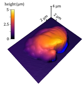
The method was demonstrated with two materials. One was a polymer film transformed by light from a rubber into a glass. Researchers found that the curing process and properties depended on exposure power and time and were spatially complex, confirming the need for fast, high-resolution measurements. The second material was a commercial 3D printing resin that changed from liquid into solid form in 12 milliseconds. A rise in resonance frequency seemed to signal polymerization and increased elasticity of the curing resin. Therefore, researchers used the AFM to make topographic images of a single polymerized voxel.
Surprising the researchers, interest in the NIST technique has extended well beyond the initial 3D printing applications. Companies in the coatings, optics and additive manufacturing fields have reached out, and some are pursing formal collaborations, NIST researchers say.
Share on:


Testimonial
"Your magazines are a great platform for people to exchange knowledge. Thank you for the work that you do."
Simon Khesin - Schmoll MaschinenSuggested Items
ITW EAE Despatch Ovens Now Support ASTM 5423 Testing
10/15/2025 | ITW EAEAs the demand for high-performance electrical insulation materials continues to grow—driven by the rapid expansion of electric vehicles (EVs) and energy storage systems—thermal processing has become a critical step in material development.
Beyond Thermal Conductivity: Exploring Polymer-based TIM Strategies for High-power-density Electronics
10/13/2025 | Padmanabha Shakthivelu and Nico Bruijnis, MacDermid Alpha Electronics SolutionsAs power density and thermal loads continue to increase, effective thermal management becomes increasingly important. Rapid and efficient heat transfer from power semiconductor chip packages is essential for achieving optimal performance and ensuring long-term reliability of temperature-sensitive components. This is particularly crucial in power systems that support advanced applications such as green energy generation, electric vehicles, aerospace, and defense, along with high-speed computing for data centers and artificial intelligence (AI).
Is Glass Finally Coming of Age?
10/13/2025 | Nolan Johnson, I-Connect007Substrates, by definition, form the base of all electronic devices. Whether discussing silicon wafers for semiconductors, glass-and-epoxy materials in printed circuits, or the base of choice for interposers, all these materials function as substrates. While other substrates have come and gone, silicon and FR-4 have remained the de facto standards for the industry.
Creative Materials to Showcase Innovative Functional Inks for Medical Devices at COMPAMED 2025
10/09/2025 | Creative Materials, Inc.Creative Materials, a leading manufacturer of high-performance functional inks and coatings, is pleased to announce its participation in COMPAMED 2025, taking place November 17–20 in Düsseldorf, Germany.
Jiva Leading the Charge Toward Sustainable Innovation
09/30/2025 | Marcy LaRont, PCB007 MagazineEnvironmental sustainability in business—product circularity—is a high priority these days. “Circularity,” the term meant to replace “recycling,” in its simplest definition, describes a full circle life for electronic products and all their elements. The result is re-use or a near-complete reintroduction of the base materials back into the supply chain, leaving very little left for waste. For what cannot be reused productively, the ultimate hope is to have better, less harmful means of disposal and/or materials that can seamlessly and harmlessly decompose and integrate back into the natural environment. That is where Jiva and Soluboard come in.