


 It’s Only Common Sense: The Phone Is Still Mightier Than the Keyboard
 The Marketing Minute: Marketing With Layers


IHEP Develops First CMOS Pixel Sensor Prototype for Circular Electron Positron Collider
October 10, 2018 | Chinese Academy of SciencesEstimated reading time: 1 minute
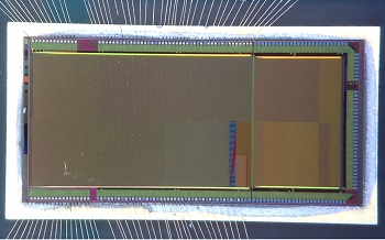
Scientists from the Institute of High Energy Physics (IHEP) have developed the first pixel sensor prototype based on the 180 nm Complementary Metal–Oxide–Semiconductor (CMOS) imaging sensor process recently. This represents significant progress in the key technology of the micro-vertex detector, the core component for the detector at the Circular Electron Positron Collider (CEPC).
CMOS pixel sensors allow integration of the sensing element and its readout electronics on the same silicon substrate, which make them attractive for charged particle tracking. The CEPC micro-vertex detector, located closest to the e+e- interaction point, will use state-of-the-art pixel technologies that provide high spatial resolution, are capable of high readout speed and adequate radiation hardness, and feature low power consumption.
The first prototype sensors, named JadePix 1, have been characterized with radioactive resources, and recently by the electron test beam at DESY in Hamburg, Germany. Preliminary results show that spatial resolutions better than 5 μm and 3.5 μm can be achieved for pixel sizes of 33×33 μm2 and 16×16 μm2, respectively. More importantly, there is no significant resolution degradation after exposure to neutron irradiation up to 1013 1 MeV neq/cm2.
The proposed Circular Electron Positron Collider (CEPC) aims at measuring Higgs properties with high precision and probing new physics beyond the Standard Model of particle physics. The CEPC Study Group has completed the conceptual design report (CDR) for the e+e- collider, and is completing the CDR for the detector. The group is pursuing an R&D program involving technologies critical for realizing the CEPC.
IHEP's Experimental Physics Division (EPD) initiated the R&D project to develop the novel CMOS pixel sensors. The advanced silicon tracking detectors and associated electronics have been the focal research direction at EPD. The division has been actively participating in several international projects, including the ATLAS Inner Tracker Upgrade, to gain design and construction experience for silicon detectors.
In addition, the division has developed pixel detectors for X-ray imaging. These detectors will soon be deployed at various stations of the High Energy Photon Source (HEPS), which will be constructed near Beijing. Meanwhile, EPD is pushing forward pixel detector R&D for the CEPC using both CMOS and SOI technologies. The goal is to design a fully functional pixel sensor and construct a larger scale prototype detector in near future.
Share on:


Testimonial
"Our marketing partnership with I-Connect007 is already delivering. Just a day after our press release went live, we received a direct inquiry about our updated products!"
Rachael Temple - AlltematedSuggested Items
Zuken Announces ZIW Americas 2026 in Dallas
10/21/2025 | ZukenZuken USA, Inc., a global leader in electrical and electronic design automation, announced Zuken Innovation World (ZIW) Americas 2026, the company’s premier global conference dedicated to advancing the future of electrical and electronic product design. ZIW 2026 will be held June 9-11 in Dallas, Texas.
Keysight Completes Acquisition of Synopsys’ Optical Solutions Group and Ansys’ PowerArtist
10/17/2025 | Keysight Technologies, Inc.Keysight Technologies, Inc., announced the completion of its acquisitions of the Optical Solutions Group from Synopsys, Inc., and PowerArtist from Ansys, Inc.
RT-Labs Joins STMicroelectronics Partner Program to Accelerate Industrial Communication
10/16/2025 | RT-LabsRT-Labs, a leading provider of real-time software solutions for industrial automation, announces that it has joined the STMicroelectronics Partner Program to integrate its Ethernet-based industrial communication stacks into ST’s development environments and microcontroller platforms.
ASC Sunstone Circuits Adds New Options to OneQuote While Maintaining Real-Time Pricing on Core PCB Features
10/16/2025 | ASC Sunstone CircuitsASC Sunstone Circuits, a leading U.S. PCB manufacturer, today announced a significant expansion of its OneQuote online quoting tool, giving design engineers more control over complex PCB configurations — making it easier for the quote team to quickly clarify and verify specifications, reducing delays from manual quote reviews.
Analog Devices Launches ADI Power Studio™ and New Web-Based Tools
10/14/2025 | Analog Devices, Inc.Analog Devices, Inc., a global semiconductor leader, announced the launch of ADI Power Studio, a comprehensive family of products that offers advanced modeling, component recommendations and efficiency analysis with simulation. In addition, ADI is introducing early versions of two new web-based tools with a modernized user experience under the Power Studio umbrella: