


 It’s Only Common Sense: The Phone Is Still Mightier Than the Keyboard
 The Marketing Minute: Marketing With Layers


Novel Topological Insulator
October 12, 2018 | University of WurzburgEstimated reading time: 2 minutes
Topological insulators are materials with very special properties. They conduct electricity or light particles on their surface or edges only but not on the inside. This unusual behaviour could eventually lead to technical innovations which is why topological insulators have been the subject of intense global research for several years.
Physicists of Julius-Maximilians-Universität Würzburg (JMU) in Bavaria, Germany, with colleagues from the Technion in Haifa, Israel, and Nanyang Technological University in Singapore now report their discovery in the journal "Nature". For the first time, the team has successfully built a topological insulator operating with both light and electronic excitations simultaneously, called an “exciton-polariton topological insulator”.
Novelty With Dual Benefit
According to Professor Sven Höfling, who heads the JMU Chair for Applied Physics, such topological insulators have a dual benefit: "They could be used for both switched electronic systems and laser applications." The topological insulators developed previously are based on either electrons or photons, allowing only one of these applications to be implemented.
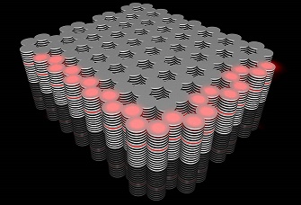
Dr. Sebastian Klembt, group leader at Höfling's chair, played a lead role in the project. He gives more details: The novel topological insulator was built on a microchip and basically consists of the gallium arsenide semiconductor compound. It has a honeycomb structure and is made up of many small pillars, each two micrometres (two millionths of a metre) in diameter.
Propagation Direction Can be Controlled
When exciting this microstructure with laser light, light-matter particles form inside it, exclusively at the edges. The particles then travel along the edges and around the corners with relatively low loss. "A magnetic field enables us to control and reverse the propagation direction of the particles," Klembt says.
It is a sophisticated systems which works in application-oriented dimensions – on a microchip – and in which light can be controlled. Usually, this is not so easy to accomplish: Pure light particles have no electric charge and therefore cannot be readily controlled with electric or magnetic fields. The new topological insulator in contrast is capable of doing this by "sending light around the corner" in a manner of speaking.
JMU and Technion: Expertise in Topological Insulators
This research success of Höfling's team shows once more that the University of Würzburg's Institute of Physics is a leading center of topological insulator research. In 2007, JMU Professor of Physics, Laurens Molenkamp, pioneered the field by experimentally building the world’s first topologically insulator. The Würzburg physicists' excellence in this field was again recognized recently in September 2018 with the awarding of a grant for the Excellence Cluster "Complexity and Topology in Quantum Materials" within the scope of the German "Excellence Strategy" competition.
The Technion scientists have complementary expertise: it is the group of Mordechai (Moti) Segev which has demonstrated the first photonic topological insulator, back in 2013, and launched the field of “Topological Photonics”. The groups have now joined forces to demonstrate this first symbiotic light-matter topological insulator, which holds great promise both as a fundamental discovery and by opening the door for exiting applications in optoelectronics.
Share on:


Testimonial
"We’re proud to call I-Connect007 a trusted partner. Their innovative approach and industry insight made our podcast collaboration a success by connecting us with the right audience and delivering real results."
Julia McCaffrey - NCAB GroupSuggested Items
Rules of Thumb: Design007 Magazine, November 2024
11/11/2024 | I-Connect007 Editorial TeamRules of thumb are everywhere, but there may be hundreds of rules of thumb for PCB design. They’re built on design formulas, fabricators’ limitations, and tribal knowledge. And unfortunately, some longtime rules of thumb should be avoided at all costs. How do we separate the wheat from the chaff, so to speak?
Connect the Dots: Best Practices for Prototyping
09/21/2023 | Matt Stevenson -- Column: Connect the DotsPCB prototyping is a critical juncture during an electronic device’s journey from concept to reality. Regardless of a project’s complexity, the process of transforming a design into a working board is often enlightening in terms of how a design can be improved before a PCB is ready for full production.
The Drive Toward UHDI and Substrates
09/20/2023 | I-Connect007 Editorial TeamPanasonic’s Darren Hitchcock spoke with the I-Connect007 Editorial Team on the complexities of moving toward ultra HDI manufacturing. As we learn in this conversation, the number of shifting constraints relative to traditional PCB fabrication is quite large and can sometimes conflict with each other.
Asia/Pacific AI Spending Surge to Reach a Projected $78 Billion by 2027
09/19/2023 | IDCAsia/Pacific spending on Artificial Intelligence (AI) ), including software, services, and hardware for AI-centric systems will grow to $78.4 billion in 2027, according to International Data Corporation's latest Worldwide Artificial Intelligence Spending Guide.
Intel to Sell Minority Stake in IMS Nanofabrication Business to TSMC
09/13/2023 | IntelIntel Corporation announced that it has agreed to sell an approximately 10% stake in the IMS Nanofabrication business to TSMC. TSMC’s investment values IMS at approximately $4.3 billion, consistent with the valuation of the recent stake sale to Bain Capital Special Situations.