


 It’s Only Common Sense: The Phone Is Still Mightier Than the Keyboard
 The Marketing Minute: Marketing With Layers


Caltech Startup Aims to Make Solar Panels More Efficient
October 19, 2018 | CaltechEstimated reading time: 3 minutes
Technology developed at Caltech seeks to improve the efficiency of solar panels by tweaking the architecture of the metal-grid layout of individual cells.
The technology, which is being marketed by a new startup company—ETC Solar, LLC—could potentially improve the output of solar panels by about 5 percent, regardless of the type of photovoltaic material used to make the panels. The translational technology was developed in the engineering and applied science lab of Harry Atwater, Howard Hughes Professor of Applied Physics and Materials Science and director of the Joint Center for Artificial Photosynthesis (JCAP). JCAP is a U.S. Department of Energy (DOE) Innovation Hub that aims to find new and effective ways to produce fuels using only sunlight, water, and carbon dioxide.
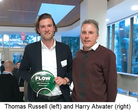
On June 28, ETC Solar took first place at the DOE's 2018 Cleantech University Prize national collegiate business plan competition in Houston.
"To have been selected as a winner is a huge point of validation for the concept, both the innovation and also the impact," says Atwater, who is also a co-founder of ETC Solar. "It has helped us to make contacts with potential industrial partners and private equity investors,"
Other co-founders of ETC Solar include Atwater group member Thomas Russell, and Rebecca Saive, assistant professor at the University of Twente in the Netherlands and a visiting associate in Atwater's lab. The company beat out 22 other teams for the top prize of $50,000 with a simple solution to a longstanding problem in solar panel technology.
When sunlight strikes solar cells, it excites electrons in the cells that are then collected via a grid of metal filaments. This grid is printed on top of the solar cells, much like the circuits on a circuit board. Tiny though the filaments may be, they do cast a shadow on the surface of the solar cell, and this shadow reduces the overall efficiency with which the cell produces energy. ETC's design uses metal filaments that have a triangular-shaped cross-section, like a steep A-frame house roof. Instead of casting a shadow on the surface of the solar panel, the filaments reflect light toward the surface. The result is a so-called "effectively transparent contact," or ETC.
The ETCs, which measure about 15 microns high, are created by direct-etching grooves into a silicon wafer. The wafer is used to fabricate a mold that is placed onto a solar panel, and the grooves are then filled with a conductive ink. Once the ink cures, the mold can be peeled off, leaving the silver ETCs behind.
ETC Solar qualified for the Cleantech competition earlier this year by winning the regional FLOW competition, run by Caltech's Resnick Sustainability Institute (RSI). The company received a grant from RSI's Rocket Fund program, supported by six California utilities and San Diego-based Moxie Foundation, that helped accelerate the technology toward commercialization. The team's business plan was also honed through the National Science Foundation (NSF) I-Corps program, which provides scientists and engineers with resources to explore the commercialization of technology developed in academia. Caltech, USC, and UCLA received a $3.5 million grant in 2014 to establish an I-Corps "node," or hub, in Southern California.
Through the I-Corps program, representatives from ETC Solar traveled around the world, conducting 150 interviews with potential customers such as solar-cell manufacturers about the commercial needs of the solar-cell market. Those interviews revealed that the biggest problems faced by manufacturers relate to efficiency and cost, as the market has incredibly tight profit margins and is driven by market-share expansion.
"Manufacturers don't adopt early technologies that easily because they say, 'Well, my margins are so low I don't have room to take financial risks,'" Russell says.
Working with Caltech's Office of Technology Transfer and Corporate Partnerships (OTTCP), Russell and his colleagues have attempted to overcome this hurdle by making the technology as market-ready as possible.
A prototype version of the ETC is expected to be completed in early 2019, when testing with industry partners will begin.
The research that led to the creation of the ETC was supported in part by the Engineering Research Center Program of the NSF; and in part by the DOE though the Office of Energy Efficiency and Renewable Energy and the Bay Area Photovoltaic Consortium.
Share on:


Testimonial
"In a year when every marketing dollar mattered, I chose to keep I-Connect007 in our 2025 plan. Their commitment to high-quality, insightful content aligns with Koh Young’s values and helps readers navigate a changing industry. "
Brent Fischthal - Koh YoungSuggested Items
Circus SE Set for High-Volume Market Entry in the Defense Sector
10/17/2025 | BUSINESS WIRECircus SE a global technology leader in AI robotics for autonomous nutrition systems and troop supply, is expanding its global production network as part of its high-volume market entry into the defense sector.
China Expands Rare Earth Export Restrictions, Tightening Grip on Global Supply Chains
10/16/2025 | I-Connect007 Editorial TeamChina sharply expanded its rare earth export restrictions on Oct. 9, adding additional elements and refining technologies to its control list while imposing stricter rules on foreign users in the defense and semiconductor industries.
SAMI Advanced Electronics Company Launches “Remal” Computer Manufacturing Project in Partnership with HP and Foxconn
10/15/2025 | SAMI-AECSAMI Advanced Electronics Company (SAMI-AEC), a wholly owned subsidiary of Saudi Arabian Military Industries (SAMI), proudly announced the launch of the “Remal” project for computer manufacturing, in strategic partnership with HP and Foxconn.
The Right Approach: Electro-Tek—A Williams Family Legacy, Part 1
10/15/2025 | Steve Williams -- Column: The Right ApproachThere is no bronze bust in the lobby or portrait in the conference room of Electro-Tek's founder—my Dad, Charles “Chuck” Williams—so with the facility closing last year after 56 years, I feel it is time to tell the story. Chuck Williams founded Electro-Tek in 1968 in our basement, eventually moving into the second floor of an old 1913 building in downtown Milwaukee that is still standing (the first of three eventual facilities).
LPKF Joins productronica’s 50th Anniversary, Showcasing Laser Technology for Electronics Manufacturing
10/10/2025 | LPKF Laser & ElectronicsLPKF Laser & Electronics invites visitors to productronica 2025 in Munich from November 18 to 21. At booth 305 in hall B2, the company will present its portfolio of modern laser technologies for the electronics industry live – from prototyping systems and high-performance depaneling to laser plastic welding for electronic housings and thin glass processing for advanced packaging.