


 It’s Only Common Sense: The Phone Is Still Mightier Than the Keyboard
 The Marketing Minute: Marketing With Layers


Graphene Printing Technique 'Silk Screens' Flexible Electronics
October 22, 2018 | IEEEEstimated reading time: 4 minutes
Future high-efficiency solar cells molded to the surface of a car; ultra-small photonics chips; and low-power, long-lasting wearable devices will all require something no one’s yet been able to achieve, namely chips made from high-efficiency materials that are flexible, thin and inexpensive to manufacture.
A research group at MIT has announced a couple of developments in recent weeks that bring such a confluence of innovations closer to the achievable. Jeehwan Kim’s research group announced separately this month in Nature Materials and Science that they can inexpensively mass-produce ultra-thin gallium arsenide and gallium nitride chips as well as a harvest the monolayer materials necessary for manufacturing other 2-D electronics like tiny photonics devices.
“We [found] the way to go to expensive semiconducting materials so you can keep producing high-quality, high-performance semiconductors with a cheaper price,” says Kim, associate professor of mechanical engineering and materials science at MIT. “The bonus is you can have flexible semiconducting devices, and because they’re really thin, you can stack them up.”
As Spectrum reported last year, Kim’s group essentially uses graphene sheets as nano-sized silk screens through which expensively manufactured exotic material-based semiconductors can be laid down.
The recipe: Take a costly, manufactured, ultra-thin film of pure semiconducting material like gallium arsenide and lay a single-layered sheet of graphene on top of it. Then flow atoms of gallium and arsenide over the graphene, and the intermediary sheet acts as a surface on which an identical copy of the underlying ultra-thin film is copied on top of the graphene — although how and why the process worked as well as it did had previously been unclear.
In the current work, Kim’s group has expanded and generalized their previous finding — discovering that on one hand that single atom crystals like silicon cannot be replicated by the “silk screen” technique (what the group calls remote epitaxy) but on the other hand that practically any 2D sheet or film whose molecules carry any net electric polarity to them can be mass produced via remote epitaxy.
The reason, the group discovered, is that electrically the graphene behaves as if it’s not even there, transmitting the ionic electric fields from the 2D material up to the slurry of raw materials resting on top of the graphene. The fields then guide the slurry into forming a perfect duplicate of the expensively manufactured thin film below.
Kim uses the shorthand term “copy-paste” to describe the simple and seemingly inexpensive procedure as it’s now being developed. (He admits, however, he cannot give price quotes at the moment, because they haven’t yet done an economic analysis of the process.)
“We were able to copy-paste … through graphene for many types of compound materials in the periodic table,” says Kim. “That is a big discovery. Based on that understanding, we were able to make single-crystalline, free-standing, very very thin membrane compound materials.”
Kim says his research group is working with “six major companies” in Korea, Japan and the United States to scale up the ultra-thin chip manufacturing processes they’re developing. He expects some of these technologies might only need “a couple years” before they’re potentially ready for commercial application.
The industries and product lines Kim says could find use for the remote epitaxy process include solar energy (cheap but ultra-efficient GaAs solar panels have long been a dream), photonics (layering multiple ultra thin films on top of each other, say, that each are efficient at transmitting red LED light and blue LED light), wearables (making electronics ultra flexible but also low power is a holy grail in the field) and IoT (ditto).
The group has a portfolio of published results that includes the graphene remote epitaxy process. Also in the running is another 2D material manufacturing technique, the one published in Science.
“We developed a way to handle wafer-scale two-dimensional materials with atomic precision,” Kim says. The idea is other materials that could be useful as conductors, insulators and semiconductors may not necessarily work with the graphene method. In which case, Kim’s group has a second method for peeling off individual individual atom-thick monolayers.
As they spell out in the Science paper, they discovered that other ultra-thin films that may for various reasons not work as well with remote epitaxy could still be copied in another way. Compounds like hexagonal boron nitride (attractive as a lubricant, electrical insulator or light emitter) and tungsten disulfide (another possible post-silicon solar panel material) can be flaked off into single-atom thick sheets with a process Kim’s lab calls controlled crack propagation.
The process involves growing a thick material on a wafer and then attaching the top of that material to a nickel plate. (2D films adhere more strongly to nickel.) The nickel plate can then be pulled up, in the process exfoliating a single-atom layer thick of the target material. The exfoliated 2D film can then be laid down onto a host wafer as part of that wafer’s manufacturing process.
Arbitrarily many single-atom thick layers can be laid down this way, Kim says, leading to new kinds of electronic devices that demand complex semiconducting substrates.
“There has been no way of handling this one atom-thick layer controllably,” Kim says. “That’s why industry has not been discussing using 2D materials in next-generation electronics. [But] we can just grow thick 2D material on the wafer. Then we just peel off one monolayer, then one monolayer. We can harvest a lot of 2D materials from … the wafer.”
Between remote epitaxy and controlled crack propagation, Kim says many more flexible, efficient electronic, photonic and other thin-film based technologies can now be more reliably mass-produced.
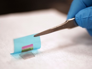
MIT researchers have devised a way to grow a single crystalline compound semiconductor on its substrate through two-dimensional materials. The compound semiconductor thin film is then exfoliated by a flexible substrate, showing the rainbow color that comes from thin film interference.
By Mark Anderson
Share on:


Testimonial
"Your magazines are a great platform for people to exchange knowledge. Thank you for the work that you do."
Simon Khesin - Schmoll MaschinenSuggested Items
ITW EAE Despatch Ovens Now Support ASTM 5423 Testing
10/15/2025 | ITW EAEAs the demand for high-performance electrical insulation materials continues to grow—driven by the rapid expansion of electric vehicles (EVs) and energy storage systems—thermal processing has become a critical step in material development.
Beyond Thermal Conductivity: Exploring Polymer-based TIM Strategies for High-power-density Electronics
10/13/2025 | Padmanabha Shakthivelu and Nico Bruijnis, MacDermid Alpha Electronics SolutionsAs power density and thermal loads continue to increase, effective thermal management becomes increasingly important. Rapid and efficient heat transfer from power semiconductor chip packages is essential for achieving optimal performance and ensuring long-term reliability of temperature-sensitive components. This is particularly crucial in power systems that support advanced applications such as green energy generation, electric vehicles, aerospace, and defense, along with high-speed computing for data centers and artificial intelligence (AI).
Is Glass Finally Coming of Age?
10/13/2025 | Nolan Johnson, I-Connect007Substrates, by definition, form the base of all electronic devices. Whether discussing silicon wafers for semiconductors, glass-and-epoxy materials in printed circuits, or the base of choice for interposers, all these materials function as substrates. While other substrates have come and gone, silicon and FR-4 have remained the de facto standards for the industry.
Creative Materials to Showcase Innovative Functional Inks for Medical Devices at COMPAMED 2025
10/09/2025 | Creative Materials, Inc.Creative Materials, a leading manufacturer of high-performance functional inks and coatings, is pleased to announce its participation in COMPAMED 2025, taking place November 17–20 in Düsseldorf, Germany.
Jiva Leading the Charge Toward Sustainable Innovation
09/30/2025 | Marcy LaRont, PCB007 MagazineEnvironmental sustainability in business—product circularity—is a high priority these days. “Circularity,” the term meant to replace “recycling,” in its simplest definition, describes a full circle life for electronic products and all their elements. The result is re-use or a near-complete reintroduction of the base materials back into the supply chain, leaving very little left for waste. For what cannot be reused productively, the ultimate hope is to have better, less harmful means of disposal and/or materials that can seamlessly and harmlessly decompose and integrate back into the natural environment. That is where Jiva and Soluboard come in.