


 It’s Only Common Sense: The Phone Is Still Mightier Than the Keyboard
 The Marketing Minute: Marketing With Layers


Special Deformation of Nanotubes to Allow them to Change Conductivity
October 23, 2018 | NUST MISISEstimated reading time: 3 minutes
Scientists from the NUST MISIS Laboratory of Inorganic Nanomaterials together with their international colleagues have proved it possible to change the structural and conductive properties of nanotubes by stretching them. This can potentially expand nanotubes’ application into electronics and high-precision sensors such as microprocessors and high-precision detectors. The research article has been published in Ultramicroscopy.
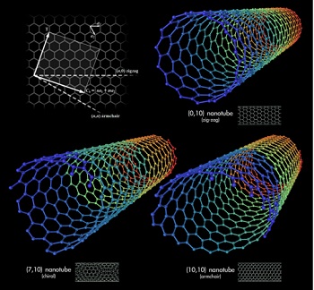
Figure 1: Different types of nanotubes: 1) zigzag, 2) chiral and 3) armchair (or dentated).
Carbon nanotubes can be represented as a sheet of graphene rolled in a special way. There are different ways of “folding” it, which leads to the graphene edges interconnecting at different angles, forming either armchair, zigzag or chiral nanotubes.
Nanotubes are considered to be promising materials for use in electronics and sensors because they have high electrical conductivity, which would work well in things like microprocessors and high-precision detectors. However, when producing carbon nanotubes, it is hard to control their conductivity. Nanotubes with metallic and semiconducting properties can grow into a single array while microprocessor-based electronics require semiconducting nanotubes that have the same characteristics.
Scientists from the NUST MISIS Laboratory of Inorganic Nanomaterials jointly with a research team from Japan, China and Australia, led by Professor Dmitri Golberg, have proposed a method that allows for the modification of the structure of ready-made nanotubes and thus changes their conductive properties.
“The basis of the nanotube — a folded layer of graphene — is a grid of regular hexagons, the vertices of which are carbon atoms. If one of the carbon bonds in the nanotube is rotated by 90° degrees, a pentagon and a heptagon are formed at this [junction] instead of a hexagon, and a so-called Stone-Wales defect is obtained in this case. Such a defect can occur in the structure under certain conditions. Back in the late 90s, it was predicted that the migration of this defect along the walls of a highly heated nanotube with the application of mechanical stress could lead to a change in its structure — a sequential change in the chirality of the nanotube, which leads to a change in its electronic properties. No experimental evidence for this hypothesis has previously been obtained, but our research paper has presented convincing proof of it”, said Associate Professor Pavel Sorokin, Doctor of Physical & Mathematical Sciences and head of the “Theoretical Materials Science of Nanostructures” infrastructure project at the NUST MISIS Laboratory of Inorganic Nanomaterials.
*Scientists from the NUST MISIS Laboratory of Inorganic Nanomaterials have conducted simulations of the experiment at the atomic level. At first, the nanotubes were lengthened to form the first structural defect consisting of two pentagons and two heptagons (a Stone-Wales defect, pic.2a), where the prolonged lengthening of the tube began to “spread” to the sides, rearranging other carbon bonds It was at this stage that the structure of the nanotubes changed. With further stretching, more and more Stone-Wales defects began to form, eventually leading to a change in the nanotubes’ conductivity.
Figure 2: The process of the nanotube structure changing: а) stretching with the first defect formation; b) the restructuring of related carbon bonds; с) the formation of new defects and the continuation of the restructuring of links.
“We were responsible for the theoretical modeling of the process on a supercomputer in the NUST MISIS Laboratory for Modeling and Development of New Materials for the experimental part of the work. We are glad that the simulation results [support] the experimental data”, added Dmitry Kvashnin, co-author of the research work, Candidate of Physical & Mathematical Sciences and a researcher at the NUST MISIS Laboratory of Inorganic Nanomaterials.
The proposed technology is capable of helping in the transformation of “metallic” nanotubes’ structure for their further application in semiconductor electronics and sensors such as microprocessors and ultrasensitive detectors.
Share on:


Testimonial
"Advertising in PCB007 Magazine has been a great way to showcase our bare board testers to the right audience. The I-Connect007 team makes the process smooth and professional. We’re proud to be featured in such a trusted publication."
Klaus Koziol - atgSuggested Items
Pulsonix 14.0 Adds Embedded Simulation, Smarter 3D Views, Enhanced Workflow
10/08/2025 | PulsonixPulsonix, the EDA company delivering technology-leading PCB design solutions, is proud to announce the launch of Pulsonix 14.0, its latest PCB design software platform.
I-Connect007 Editor’s Choice: Five Must-Reads for the Week
06/06/2025 | Nolan Johnson, I-Connect007Maybe you’ve noticed that I’ve been taking to social media lately to about my five must-reads of the week. It’s just another way we’re sharing our curated content with you. I pay special attention to what’s happening in our industry, and I can help you know what’s most important to read about each week. Follow me (and I-Connect007) on LinkedIn to see these and other updates.
INEMI Interim Report: Interconnection Modeling and Simulation Results for Low-Temp Materials in First-Level Interconnect
05/30/2025 | iNEMIOne of the greatest challenges of integrating different types of silicon, memory, and other extended processing units (XPUs) in a single package is in attaching these various types of chips in a reliable way.
Siemens Leverages AI to Close Industry’s IC Verification Productivity Gap in New Questa One Smart Verification Solution
05/13/2025 | SiemensSiemens Digital Industries Software announced the Questa™ One smart verification software portfolio, combining connectivity, a data driven approach and scalability with AI to push the boundaries of the Integrated Circuit (IC) verification process and make engineering teams more productive.
Cadence Unveils Millennium M2000 Supercomputer with NVIDIA Blackwell Systems
05/08/2025 | Cadence Design SystemsAt its annual flagship user event, CadenceLIVE Silicon Valley 2025, Cadence announced a major expansion of its Cadence® Millennium™ Enterprise Platform with the introduction of the new Millennium M2000 Supercomputer featuring NVIDIA Blackwell systems, which delivers AI-accelerated simulation at unprecedented speed and scale across engineering and drug design workloads.